
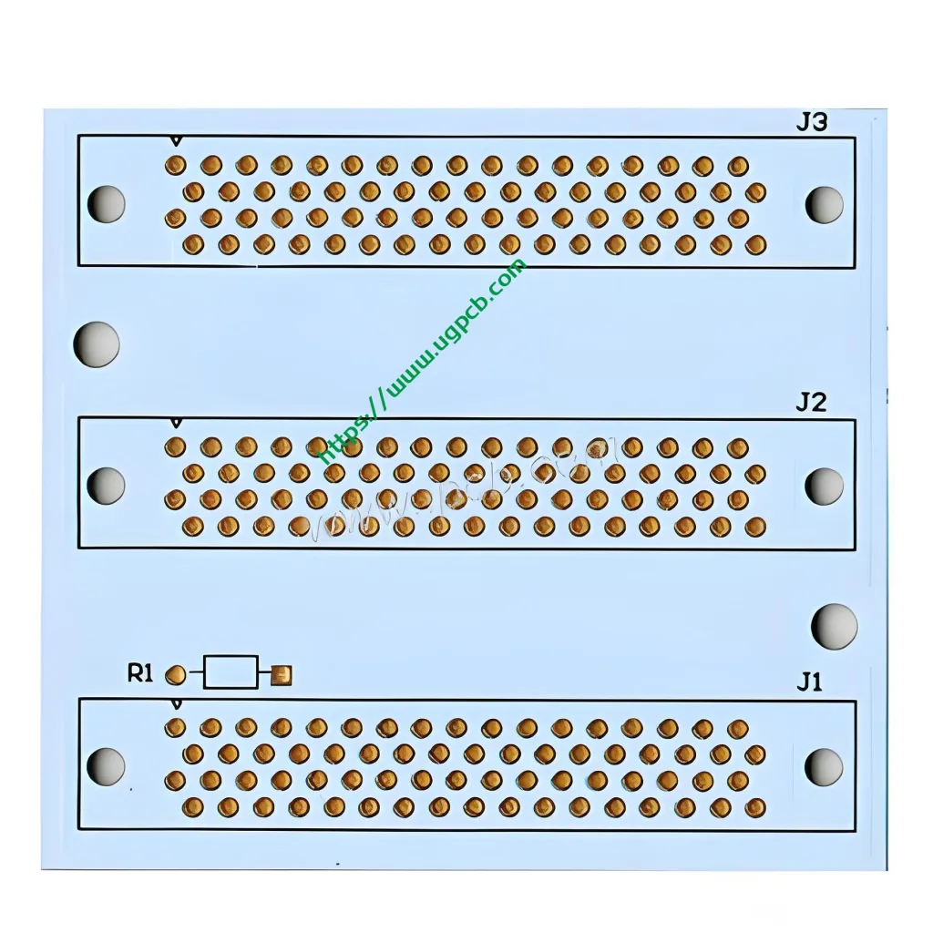
UGPCB Double-Sided PCB Product Overview
UGPCB’s double-sided PCB is a high-performance プリント基板 specifically engineered for electronic devices such as adapters. Constructed with FR-4材, it features a standard thickness of 1.6mm, 1 OZ銅の厚さ, and Immersion Gold (同意する) 表面仕上げ. The minimum trace width and spacing are both 6 ミル (0.15mm). By facilitating circuit routing on both sides of the substrate, double-sided PCBs enable higher wiring density and enhanced reliability, making them extensively applicable in various PCB アセンブリ (プリント基板) プロジェクト. As a leader in the PCB industry, UGPCB is dedicated to delivering high-quality PCB manufacturing services, assisting customers in optimizing electronic designs and improving overall performance.
In today’s electronics sector, PCBs and PCBA are core components. 両面PCB, valued for their flexibility and cost-effectiveness, are the preferred choice for numerous projects. This guide provides an in-depth analysis of UGPCB’s double-sided PCBs, covering their definition, design essentials, 働く原則, アプリケーション, classifications, 材料, パフォーマンス, 構造, 特徴, 製造工程, and usage scenarios. It aims to offer a thorough understanding of this product and deliver reliable solutions for your PCBA projects.
Product Definition and Structure
What is a Double-Sided PCB?
A double-sided PCB is a printed circuit board with conductive copper layers on both sides of the substrate, allowing circuits on the top and bottom to be interconnected through vias or plated-through holes. This design significantly enhances PCB routing flexibility, making it suitable for moderately complex electronic devices. UGPCB’s double-sided PCB employs a 2-layer structure combined with an Immersion Gold surface finish, ensuring excellent conductivity and corrosion resistance, making it an ideal foundation for PCBA.
Structural Composition
The structure of UGPCB’s double-sided PCB comprises the substrate, 銅層, はんだマスク, and surface finish layer. The substrate utilizes FR-4 material, a glass-reinforced epoxy laminate known for its good mechanical strength and electrical insulation. The copper layers, with a thickness of 1 オンス (approximately 35μm), are distributed on both sides and interconnected via drilling and plating processes. The surface finish employs Immersion Gold technology to enhance solderability and oxidation resistance. With an overall thickness of 1.6mm, this PCB ensures stability and durability, catering to high-density PCB applications.
Key Design Considerations for Double-Sided PCBs
When designing double-sided PCBs, particular attention must be paid to trace width and spacing parameters. UGPCB’s product offers a minimum trace width and spacing of 6 ミル (0.15mm), facilitating high-density routing while mitigating signal interference and short circuits. Designers should also consider thermal management and impedance control to ensure stable PCB performance during PCBA assembly. さらに, the Immersion Gold surface finish necessitates optimized pad layouts to improve solderability and reliability. For applications like adapter PCBs, using professional プリント基板設計 software to simulate circuit performance is recommended to minimize production errors.
Working Principle of Double-Sided PCBs
The operational principle of double-sided PCBs is based on circuit interconnections on both sides of the substrate, transmitting electrical signals and power through conductive vias. As current flows through the copper traces, the PCB acts as a carrier, connecting various electronic components to achieve specific functions. 例えば, in adapter PCBs, the double-sided design allows power management circuits to be distributed on both sides, improving efficiency and thermal performance. The Immersion Gold surface finish ensures low resistance at contact points, extending the PCB’s lifespan. The entire process relies on high-quality PCBA to integrate the PCB with コンポーネント, forming a complete electronic system.
アプリケーションと分類
主要なアプリケーション
UGPCB’s double-sided PCBs are widely used in electronic devices, particularly in the adapter PCB sector for power adapters, chargers, and converters. They are also common in communication equipment, 自動車エレクトロニクス, および産業用制御システム, serving as core components in PCBA. Their high reliability and flexibility make them suitable for low to medium complexity circuits, aiding customers in achieving efficient プリント基板の製造 およびPCBAサービス.
製品分類
Based on application and performance, double-sided PCBs can be categorized into several types, including standard double-sided PCBs, 高密度相互接続 (HDI) プリント基板, and specialized adapter PCBs. UGPCB’s products fall into the latter category, optimized for adapters and supporting custom colors (例えば。, white or black) to meet diverse PCBA project requirements. Classification is based on materials, 厚さ, そして表面仕上げ, such as FR-4 PCBs and Immersion Gold PCBs.
材料とパフォーマンス
使用材料
UGPCB’s double-sided PCBs use FR-4 as the substrate material—a flame-retardant epoxy glass cloth laminate that provides excellent electrical insulation and mechanical strength. The copper layers consist of 1 oz electrolytic copper, ensuring high conductivity. The surface finish employs Immersion Gold, 耐食性とはんだ付け性の向上. This material combination ensures PCB stability in harsh environments, forming the basis for high-quality PCBA assembly.
性能特性
This PCB product boasts high reliability, excellent thermal stability, and good signal integrity. Performance parameters include high-temperature resistance, 低い誘電率, and resistance to chemical corrosion. The minimum trace width/spacing of 6 mil supports precise circuit design. The Immersion Gold treatment improves solder joint quality, reducing failure rates and ensuring outstanding performance in PCB and PCBA applications. These characteristics make it the preferred choice for scenarios like adapter PCBs.
主要な製品機能
UGPCB’s double-sided PCB offers key features such as high-density routing capability, 費用対効果, and environmental compliance. Its double-sided design allows for more complex circuit layouts, while the 1.6mm thickness and 1 oz copper weight ensure mechanical durability. The Immersion Gold surface finish provides long life and low maintenance, with the minimum 6 mil trace width/spacing supporting high-precision PCB manufacturing. さらに, white or black appearance options enhance aesthetics, making it suitable for various PCBA projects and boosting product market competitiveness.
製造工程の概要
The production process for double-sided PCBs involves multiple steps: It begins with substrate preparation and inner-layer imaging, followed by drilling to create vias, then plating and outer-layer imaging. The Immersion Gold surface finish is applied in later stages to protect the copper layers. ついに, the PCBs undergo testing and inspection before packaging and shipment. UGPCB employs advanced PCB manufacturing technologies, strictly controlling each step to provide reliable PCBA support services. The entire process is efficient and environmentally friendly, complying with international standards.

Common Usage Scenarios
UGPCB’s double-sided PCBs are used in diverse scenarios, including power adapters, 家電, 医療機器, and industrial automation. In adapter PCB applications, they are used for power conversion and distribution, ensuring safe device operation. Other scenarios, such as communication base stations and automotive electronics, rely on their high reliability and PCBA compatibility. Through optimized design, this PCB can adapt to various environments, helping customers achieve efficient electronic solutions.


