
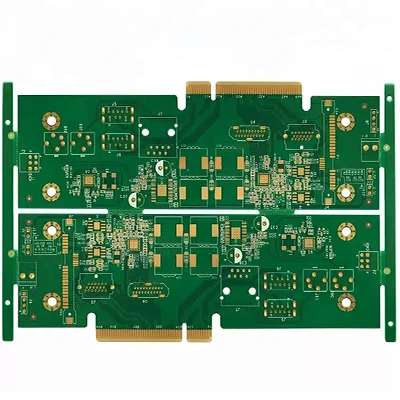
Overview of 6 Layer Golden Finger PCB
The 6 Layer Golden Finger PCB is a high-precision, multi-layered printed circuit board designed for advanced electronic applications. This product combines multiple layers of conductive traces and insulating materials to provide exceptional performance and reliability in various electronic devices.
意味
あ 6 Layer Golden Finger PCB is a type of multi-layer printed circuit board (プリント基板) that features six individual layers of conductive material, 絶縁層によって分離されています. 用語 “Golden Finger” refers to the specific surface treatment applied to the edges of the board, which involves immersion gold and additional gold plating on the contact fingers.
設計要件
When designing a 6 Layer Golden Finger PCB, several key requirements must be considered:
- 材料品質: High-quality FR4 material is essential for durability and performance.
- レイヤー構成: Six layers are needed to accommodate complex circuitry and signal routing.
- 銅の厚さ: A standard copper thickness of 1OZ ensures adequate conductivity.
- 表面処理: Immersion gold with additional gold finger plating enhances connectivity and corrosion resistance.
- トレース/スペースの寸法: A minimum trace/space of 4mil/4mil is required for precise circuit patterns.
- 特別なプロセス: The gold finger process with a thickness of 0.1um is critical for reliable edge connections.
作業原則
The 6 Layer Golden Finger PCB operates based on the principles of electrical conductivity and insulation. Conductive traces on different layers create pathways for electrical signals, 一方、絶縁層は、これらの信号間の不要な相互作用を防ぎます. The gold finger edges facilitate easy insertion into connectors, ensuring stable and reliable connections.
アプリケーション
This type of PCB is widely used in applications that require high precision and reliability, のような:
- High-speed digital circuits
- 通信機器
- Advanced computing systems
- 自動車電子機器
- 医療機器
分類
6 Layer Golden Finger PCBs can be classified based on their intended use, のような:
- 信号処理ボード: 通信デバイスの高周波信号を処理するため.
- 配電板: 複雑な電子システムの電源を管理するため.
- コントロールボード: For controlling and managing various functions in electronic devices.
材料
The primary materials used in the construction of a 6 Layer Golden Finger PCB include:
- 基本材料: FR4, 優れた誘電特性と機械的強度で知られている火炎耐性繊維グラスファイバー材料材料.
- 導電性材料: 銅, 導電性トレースに使用されます.
- 表面処理: Immersion gold and additional gold plating for the gold fingers.
パフォーマンス
のパフォーマンス 6 Layer Golden Finger PCB is characterized by:
- 高い信号の完全性: 正確なトレース/スペースの寸法と高品質の素材のため.
- 信頼できる接続: Ensured by the gold finger surface treatment.
- 耐久性: Enhanced by the robust FR4 base material and immersion gold finish.
- 電気効率: 最適化されたレイヤー構成による信号損失と干渉の最小化.
構造
The structure of a 6 Layer Golden Finger PCB consists of:
- 導電性材料の6層: 絶縁層と交互に.
- Gold Finger Edges: Plated with a thin layer of gold for enhanced connectivity.
- Protective Layers: Including solder mask and silkscreen for protection and identification.
特徴
Key features of the 6 Layer Golden Finger PCB include:
- 高度な表面処理: Immersion gold plus gold finger for superior connection quality.
- 高精度: With a minimum trace/space of 4mil/4mil.
- カスタマイズ可能なカラーオプション: 緑または白からお選びいただけます.
- 標準の厚さ: 完成した厚さは1.6mmです.
製造工程
The production process for a 6 Layer Golden Finger PCB involves several steps:
- 材料の準備: FR4シートと銅ホイルの選択と準備.
- レイヤースタッキング: 銅と断熱材の交互の層.
- エッチング: 過剰な銅を除去して、目的の回路パターンを形成します.
- メッキ: Applying immersion gold and additional gold finger plating.
- ラミネート加工: 熱と圧力の下で層を組み合わせます.
- 掘削: スルーホールコンポーネントとVIAの穴を作成します.
- ソルダーマスクの塗布: はんだブリッジと環境要因から回路を保護します.
- シルクスクリーン印刷: コンポーネントの配置と識別のためのテキストとシンボルを追加します.
- 品質管理: PCBがすべての設計仕様と標準を満たすようにします.
シナリオを使用します
The 6 Layer Golden Finger PCB is ideal for scenarios where:
- 高い信号の完全性が重要です.
- 信頼できる耐久性のある接続が必要です.
- スペースの制約により、コンパクトで効率的な設計が必要です.
- パフォーマンスを向上させるには、高度な表面処理が必要です.


