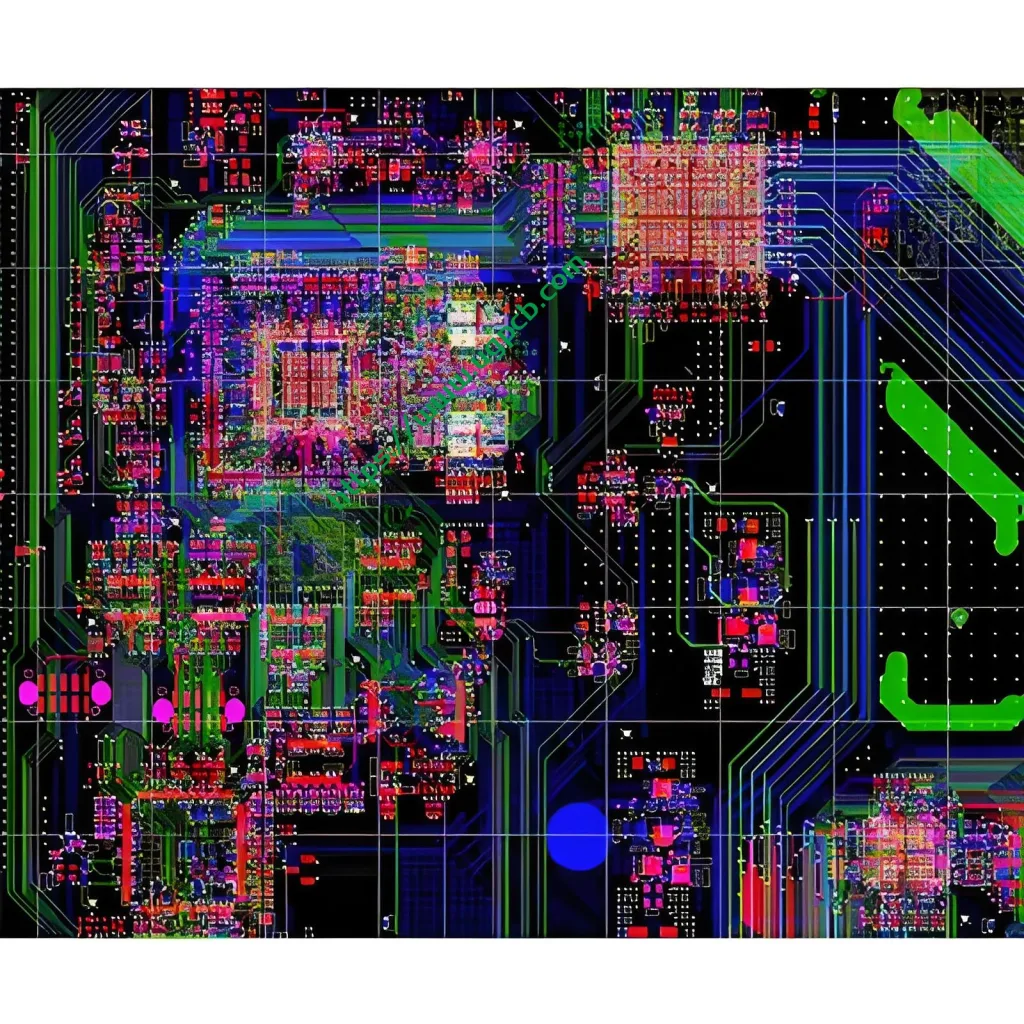
高速および高密度PCBA設計 名前: 高速および高密度PCBA設計 皿: TG170 /TG180, F4BM, FR4, FR1-4, 等. 設計可能なレイヤー: 1-32 レイヤー 最小ライン幅とライン間隔: 3ミル 最小レーザーアパーチャ: 4ミル 最小機械的開口: 8ミル 銅箔の厚さ: 18-175cm (標準: 18CM35CM70cm) 皮の強度: 1.25N/mm 最小パンチングホールの直径: 片側: 0.9mm/35mil 最小穴の直径: 0.25mm/10mil 開口耐性: ≤φ0.8mm±0.05mm お問い合わせを送信 すぐに見積もりを取得 製品詳細 高速PCB設計の定義 要するに, 高速PCB設計は、ボードの物理的特性によって信号の整合性が影響を受けるデザインです. 重要な物理的特性 レイアウト 包装 レイヤースタッキング 相互接続 共有: フェイスブックツイッターリンクトインワッツアップ 前へ: 14-レイヤー25G高速HDI PCB設計 次: 12-層の自動車高速バックプレーン設計 関連製品 24-高密度高速PCBを層にします 12-層の自動車高速バックプレーン設計 14-レイヤー25G高速HDI PCB設計 高速サーバーバックプレーンPCB設計 通信端子回路基板の設計 5G通信回路基板の設計 人工知能回路基板の設計 高周波高速PCB設計 人気の製品 レーダー基板 ロジャース基板 ISOLA 370HR 基板 テフロン高周波基板 12L3+N+3 HDIボード HDI マウスバイト PCB メーカー | 高密度相互接続ボード