バックプレーンの概要
バックプレーンは、高速設計の要素を組み込んだ高度な回路基板です, 機械設計, 高電圧/高電流デザイン, また、RFデザイン.
バックプレーンのアプリケーション
防衛システム
これらのボードは、ミッションクリティカルな防御システムで一般的に使用されています.
通信システム
バックプレーンは、通信システムでも利用されています.
データセンター
さらに, 彼らはデータセンターで重要な役割を果たします.

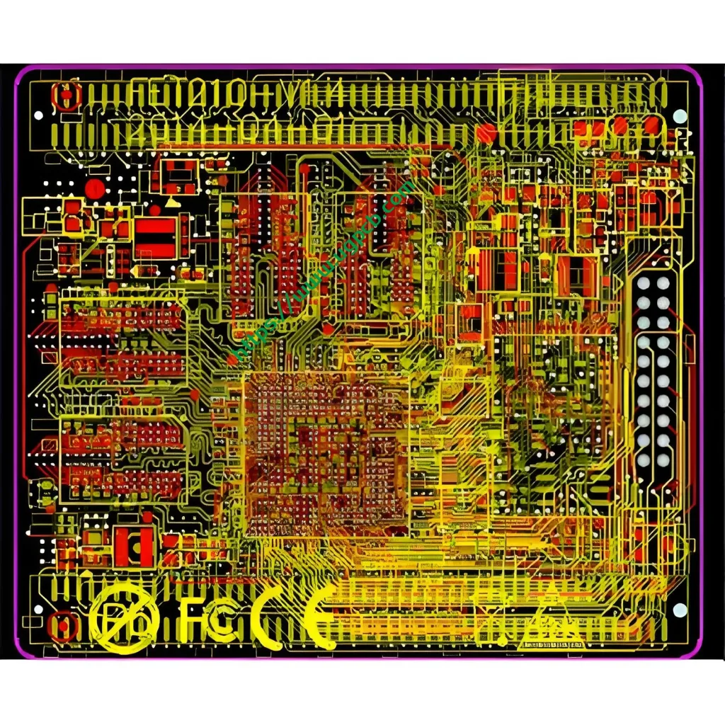
バックプレーンは、高速設計の要素を組み込んだ高度な回路基板です, 機械設計, 高電圧/高電流デザイン, また、RFデザイン.
これらのボードは、ミッションクリティカルな防御システムで一般的に使用されています.
バックプレーンは、通信システムでも利用されています.
さらに, 彼らはデータセンターで重要な役割を果たします.
前へ: 通信端子回路基板の設計

WeChat で QR コードをスキャンします


