Overview of LCD
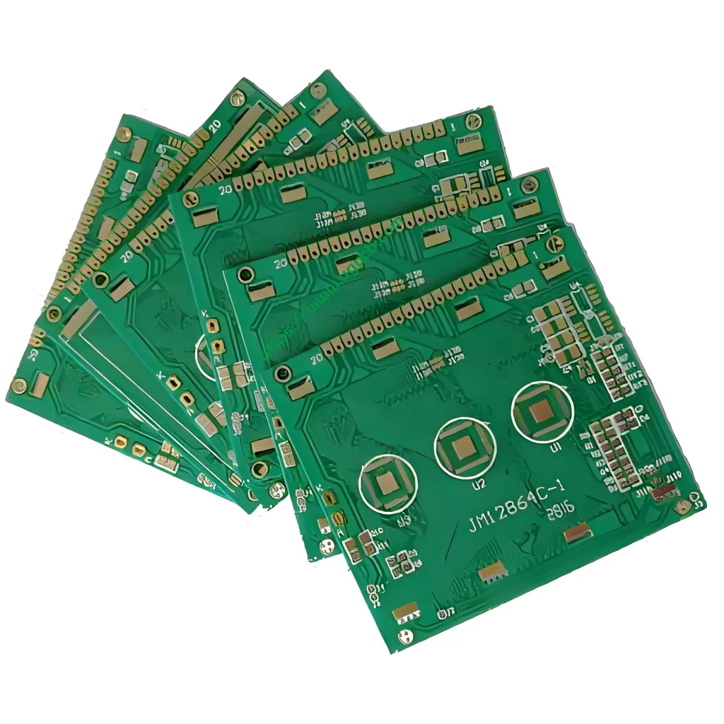
LCD – liquid crystal display, つまり, the display. LCD is a typical three-layer structure used in various electronic devices.
Structure of LCD
LCD is a typical three-layer structure in which the liquid crystal is placed between two parallel sheets of glass.
Components of LCD Structure
- Glass Sheets: Two parallel sheets of glass serve as the foundation.
- Crystal Molecules: Between the two pieces of glass, there are many small vertical and horizontal lines. The rod-shaped crystal molecules are crucial for display functionality.
Functionality of LCD
The direction of the rod-shaped crystal molecules is changed by a voltage. This change causes the light to refract, and subsequently, the picture is displayed.
Mechanism of Display
- Voltage Application: Applying a voltage alters the direction of the crystal molecules.
- Light Refraction: The altered direction of the molecules refracts light, resulting in the display of an image.
 UGPCBのロゴ

