
多層GPSモジュールPCBの概要
マルチレイヤーGPSモジュールPCBは、GPSモジュールアプリケーションの厳しい要件を満たすように設計された専門製品です. このタイプの プリント基板 高い精度を提供します, 信頼性, とパフォーマンス, さまざまなナビゲーションおよびポジショニングシステムに理想的な選択肢になる.
意味
GPSモジュール用の多層PCBはaです プリント基板 GPSモジュールの機能をサポートするように特別に設計されています. 導電性と断熱材の複数の層で構成されています, GPSモジュールの動作に不可欠な複雑な電気経路と接続を提供する.
設計要件
GPSモジュール用に多層PCBを設計するとき, いくつかの重要な要件を満たす必要があります:
- 材料品質: 高品質のFR4材料は、耐久性と信号の完全性に不可欠です.
- レイヤー構成: 4層の設計が標準です, 複雑な回路と信号ルーティングを可能にします.
- 銅の厚さ: 1オンスの銅の厚さは、適切な導電率を保証します.
- 表面処理: 浸漬金表面処理により、接続性と耐食性が向上します.
- トレース/スペースの寸法: 4milの最小トレースとスペースの寸法 (0.1mm) 正確な回路パターンに必要です.
- 特別な機能: ハーフホール プリント基板設計 多くの場合、特定のコンポーネントの配置とはんだ付けの要件に組み込まれています.
作業原則
GPSモジュール用の多層PCBは、電気伝導率と断熱の原理に基づいて動作します. 導電性層は、電気信号の経路を形成します, 一方、絶縁層は、これらの信号間の不要な相互作用を防ぎます. 浸漬金表面処理は優れた接続性を提供し、環境要因から保護します.
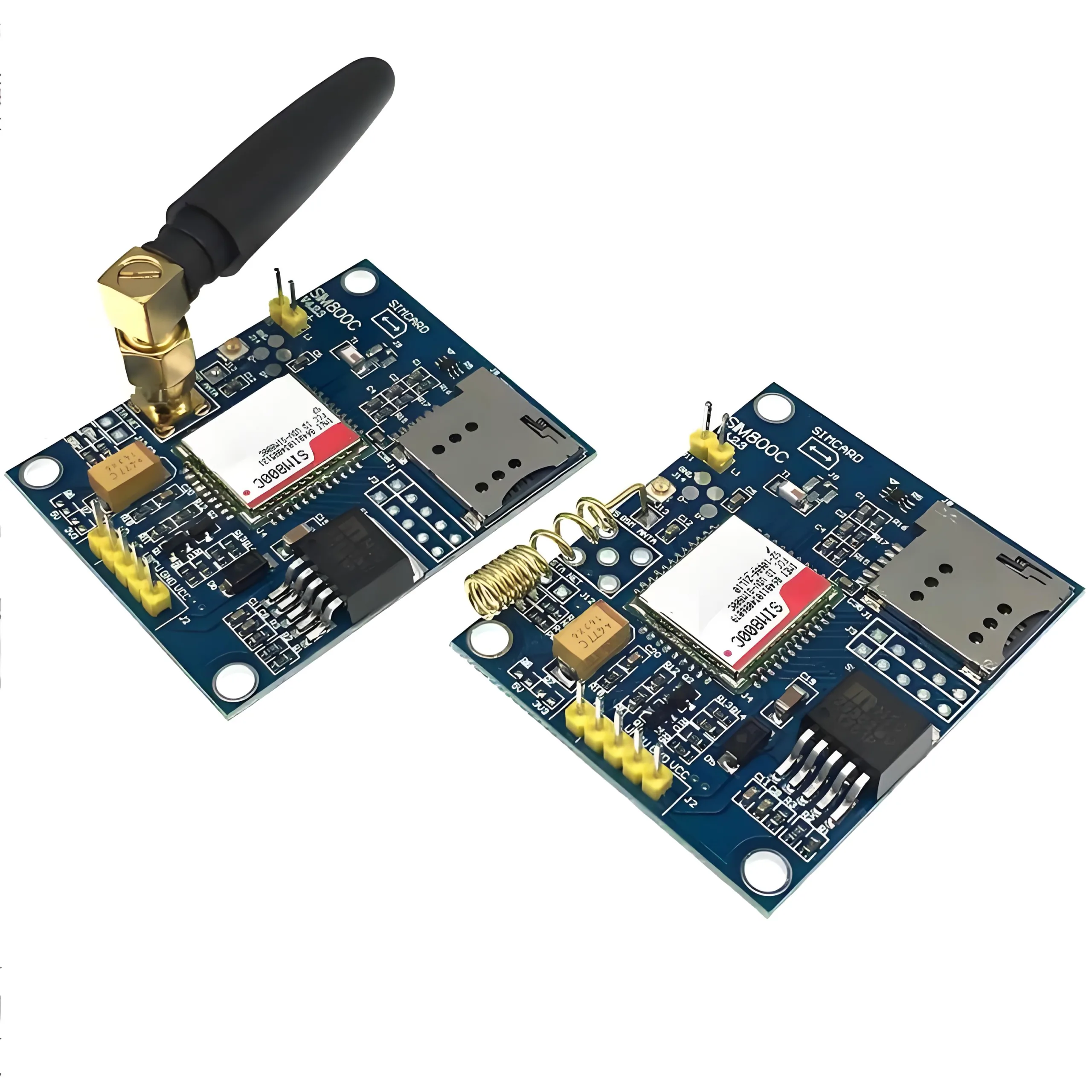
アプリケーション
このタイプのPCBは、主にGPSモジュールで使用されています, これは、などのさまざまなアプリケーションで重要なコンポーネントです:
- ナビゲーションシステム
- ポジショニングデバイス
- 通信機器
- 自動車電子機器
- 海洋ナビゲーションシステム
分類
GPSモジュール用の多層PCBは、その特定の機能と意図した使用に基づいて分類できます, のような:
- 信号処理ボード: 通信デバイスの高周波信号を処理するため.
- コントロールボード: 電子システムのさまざまな機能を管理および制御するため.
- 配電板: 複雑な電子システムの電源を管理するため.
材料
GPSモジュール用の多層PCBの構築に使用される主要な材料は含まれます:
- 基本材料: FR4, 優れた誘電特性と機械的強度で知られている火炎耐性繊維グラスファイバー材料材料.
- 導電性材料: 銅, 導電性トレースに使用されます.
- 表面処理: イマージョンゴールド, 接続を向上させ、耐食性を提供します.
パフォーマンス
のパフォーマンス 多層PCB GPSモジュールの場合は特徴付けられます:
- 高い信号の完全性: 正確なトレース/スペースの寸法と高品質の素材のため.
- 信頼できる接続: 浸漬金表面処理によって保証されます.
- 耐久性: 堅牢なFR4によって強化されました 基本材料.
- 電気効率: 最適化されたレイヤー構成による信号損失と干渉の最小化.
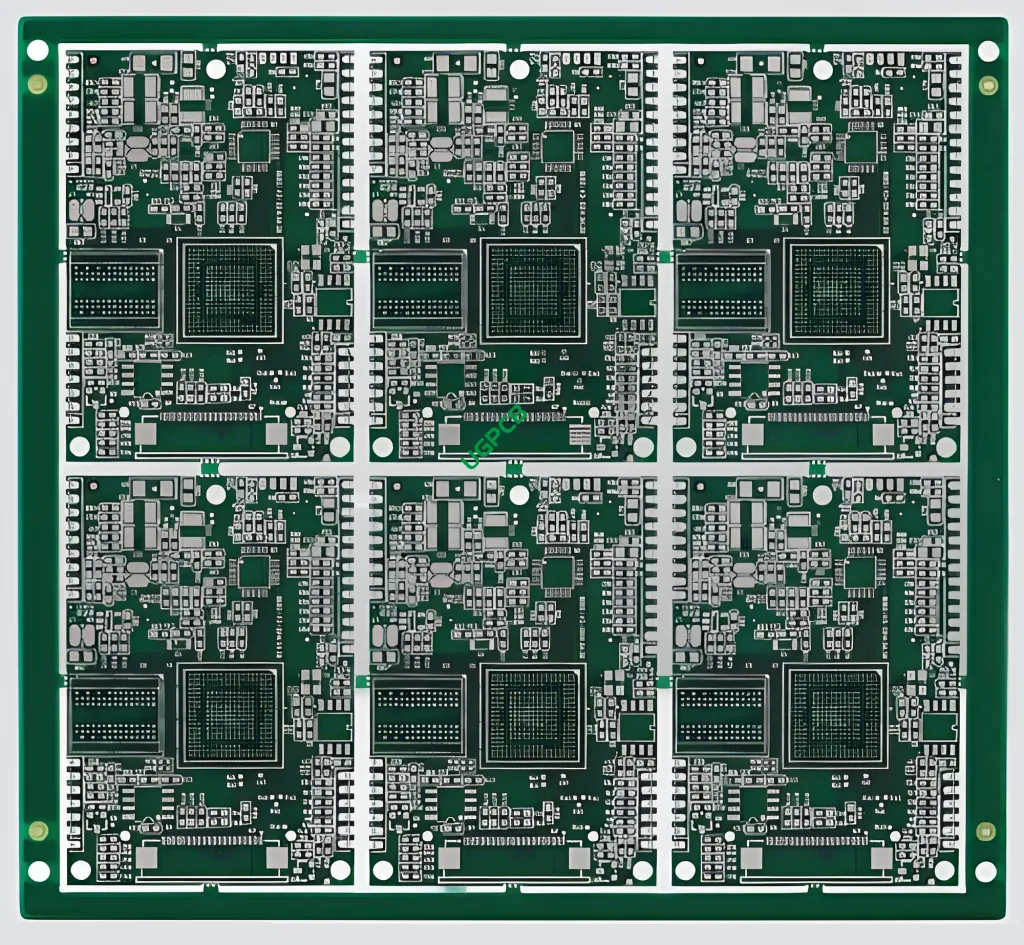
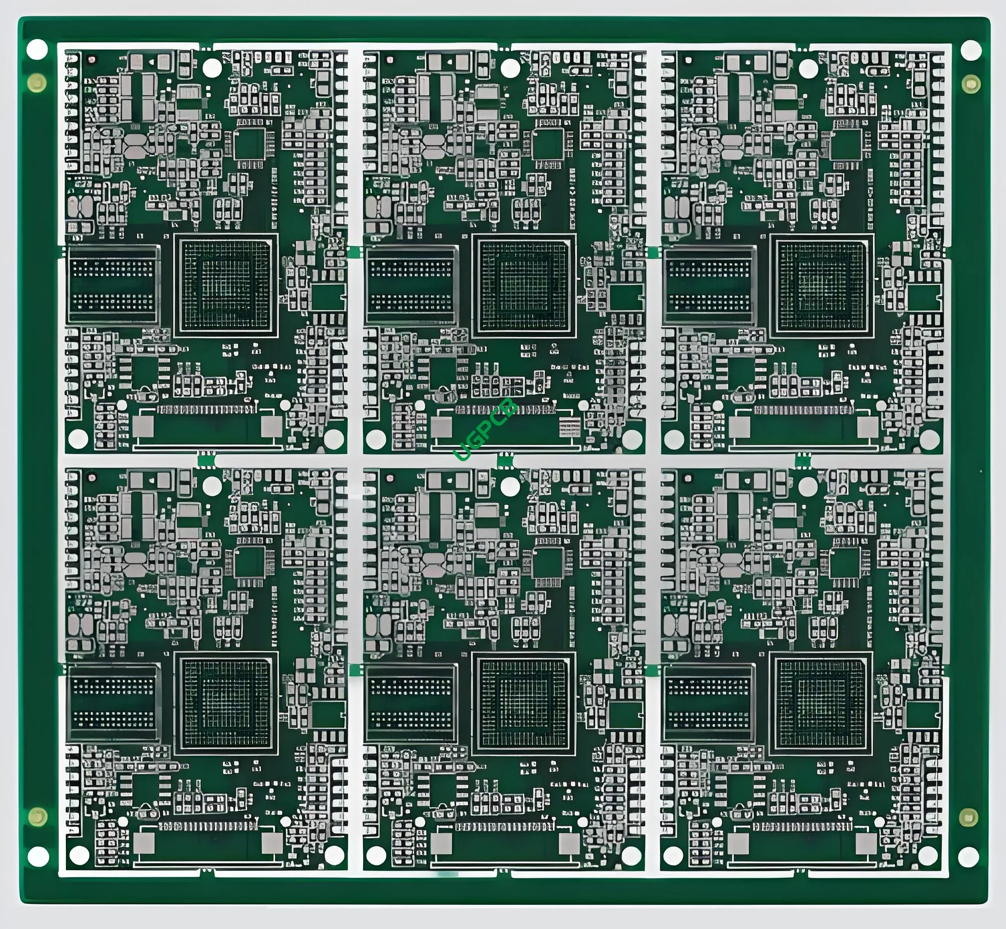
構造
GPSモジュール用の多層PCBの構造は:
- 導電性材料の4層: 絶縁層と交互に.
- 浸漬金表面処理: 強化された接続と保護のため.
- ハーフホールデザイン: 特定のコンポーネントの配置とはんだ付け要件について.
特徴
GPSモジュール用の多層PCBの主要な機能には含まれます:
- 高度な表面処理: 優れた接続品質のための浸漬金.
- 高精度: 4milの最小トレースとスペースの寸法を備えています (0.1mm).
- カスタマイズ可能なカラーオプション: 緑または白からお選びいただけます.
- 標準の厚さ: 仕上がり厚さ1.0mm.
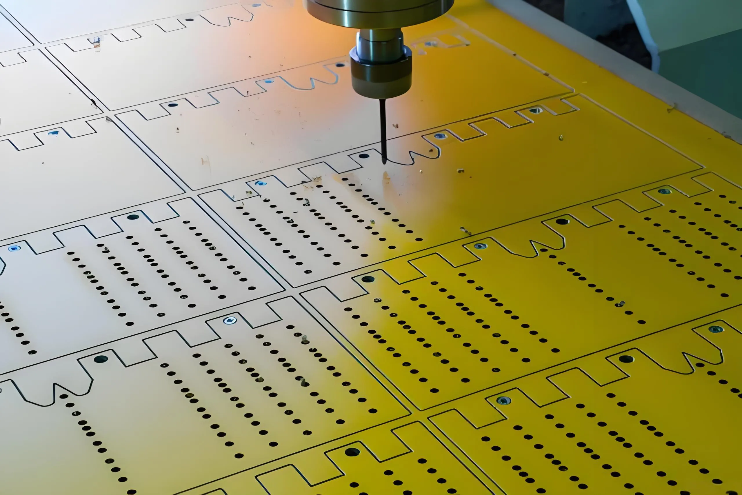
製造工程
GPSモジュール用の多層PCBの生産プロセスには、いくつかのステップが含まれます:
- 材料の準備: FR4シートと銅ホイルの選択と準備.
- レイヤースタッキング: 銅と断熱材の交互の層.
- エッチング: 過剰な銅を除去して、目的の回路パターンを形成します.
- メッキ: 浸漬金表面処理の適用.
- ラミネート加工: 熱と圧力の下で層を組み合わせます.
- 掘削: スルーホールコンポーネントとVIAの穴を作成します.
- ソルダーマスクの塗布: はんだブリッジと環境要因から回路を保護します.
- シルクスクリーン印刷: コンポーネントの配置と識別のためのテキストとシンボルを追加します.
- 品質管理: PCBがすべての設計仕様と標準を満たすようにします.
シナリオを使用します
GPSモジュール用の多層PCBは、シナリオに最適です:
- 高い信号の完全性が重要です.
- 信頼できる耐久性のある接続が必要です.
- スペースの制約により、コンパクトで効率的な設計が必要です.
- パフォーマンスを向上させるには、高度な表面処理が必要です.


