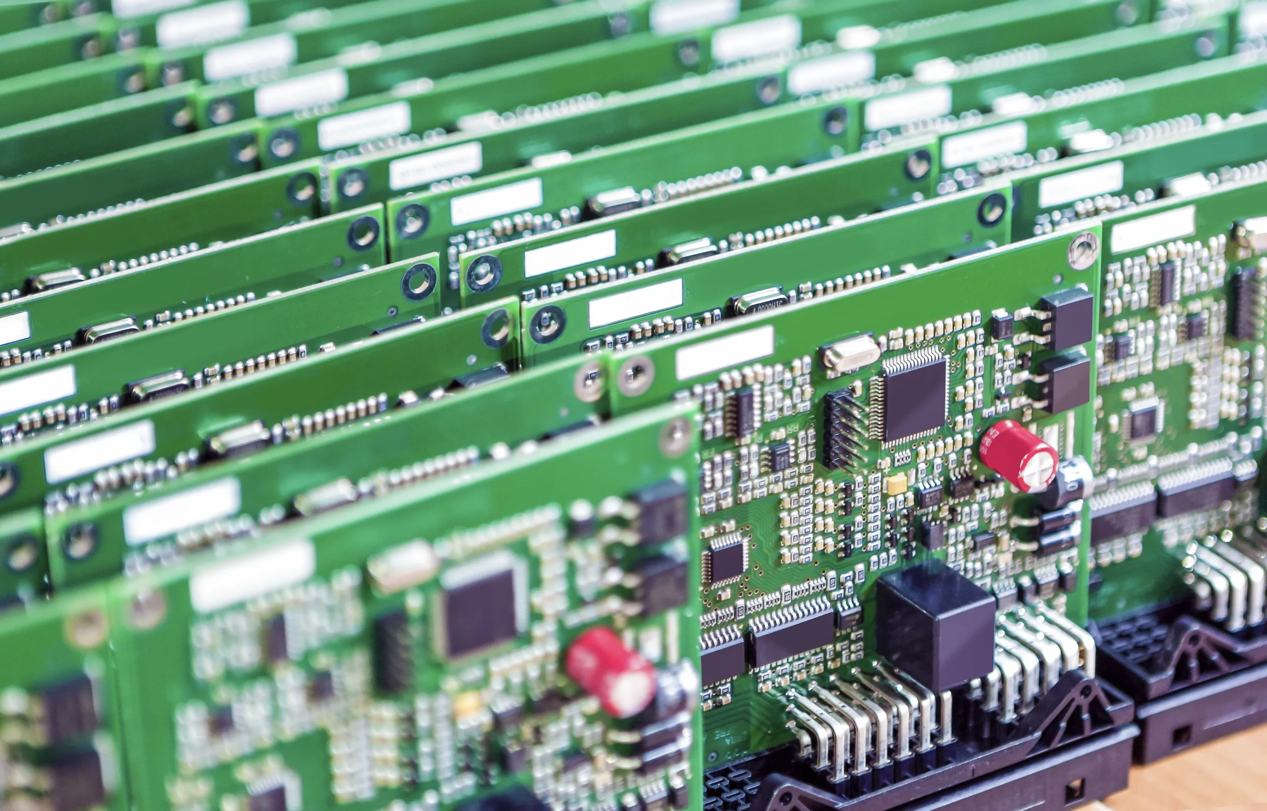
多層PCBの定義
多層 PCB は 2 層以上の回路基板です。. 両面PCBとは異なります, 導電性材料が 2 層しかない, すべての多層 PCB には、材料の中心に少なくとも 3 層の導電性材料が埋め込まれている必要があります。.
多層プリント基板の構造
異なるレイヤーの組み合わせ
名前が示すように, 多層 PCB はさまざまな層を組み合わせたものです. 片面 PCB と両面 PCB を組み合わせて、この複雑な設計の PCB を形成します. 多層 PCB では層の数が増えるため、配線に利用できる領域が増加します。. これらの基板は、2 層の PCB を組み合わせ、誘電体などの絶縁材料で分離して作られています。.
導電層の数
絶縁材間の導電層は最低 3 層です, 必要に応じて最大 100 個のレイヤーを組み込むことができます. フレキシブル多層基板は製造が難しいため、多層基板をリジッド基板として扱います。. 当社の一般的な多層 PCB のほとんどは次のもので構成されています。 4 に 8 レイヤー. スマートフォンには以下のものを入れることができます 12 アプリケーションの複雑さに合わせてレイヤーを選択します. メーカーは奇数番号のレイヤーよりも偶数番号のレイヤーを好む, 奇数の層を積層すると回路が過度に複雑になり、問題が発生する可能性があるためです。, コストが高いことも考慮すべき要素です.
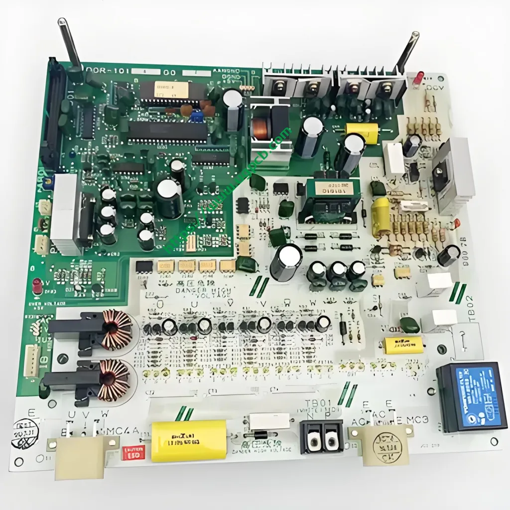
多層PCBのメリット
多層 PCB には、単層または二層 PCB に比べていくつかの利点があります。. 密度が高い, より優れた機能を可能にする, 容量と速度. 電源プレーンとグランドプレーンが正しく配置されていれば、電磁シールドが容易になります。. 大規模な配線は必要ありません, だから軽いです. サイズが小さくなり、スペースの節約に役立ちます. 他のタイプの PCB よりも柔軟性に優れています。.
多層PCBの応用例
多層 PCB には多くの用途があります. これらには含まれます:
-
コンピューター
-
光ファイバー受信機
-
データストレージ
-
信号伝送
-
携帯電話の通信
-
携帯電話中継器
-
GPSテクノロジー
-
産業管理
-
衛星システム
-
ハンドヘルドデバイス
-
試験装置
-
X線装置
-
心拍モニター
-
CATスキャン技術
-
原子加速器
-
中央火災警報システム
-
核探知システム
-
空間検知装置
-
気象分析装置


