

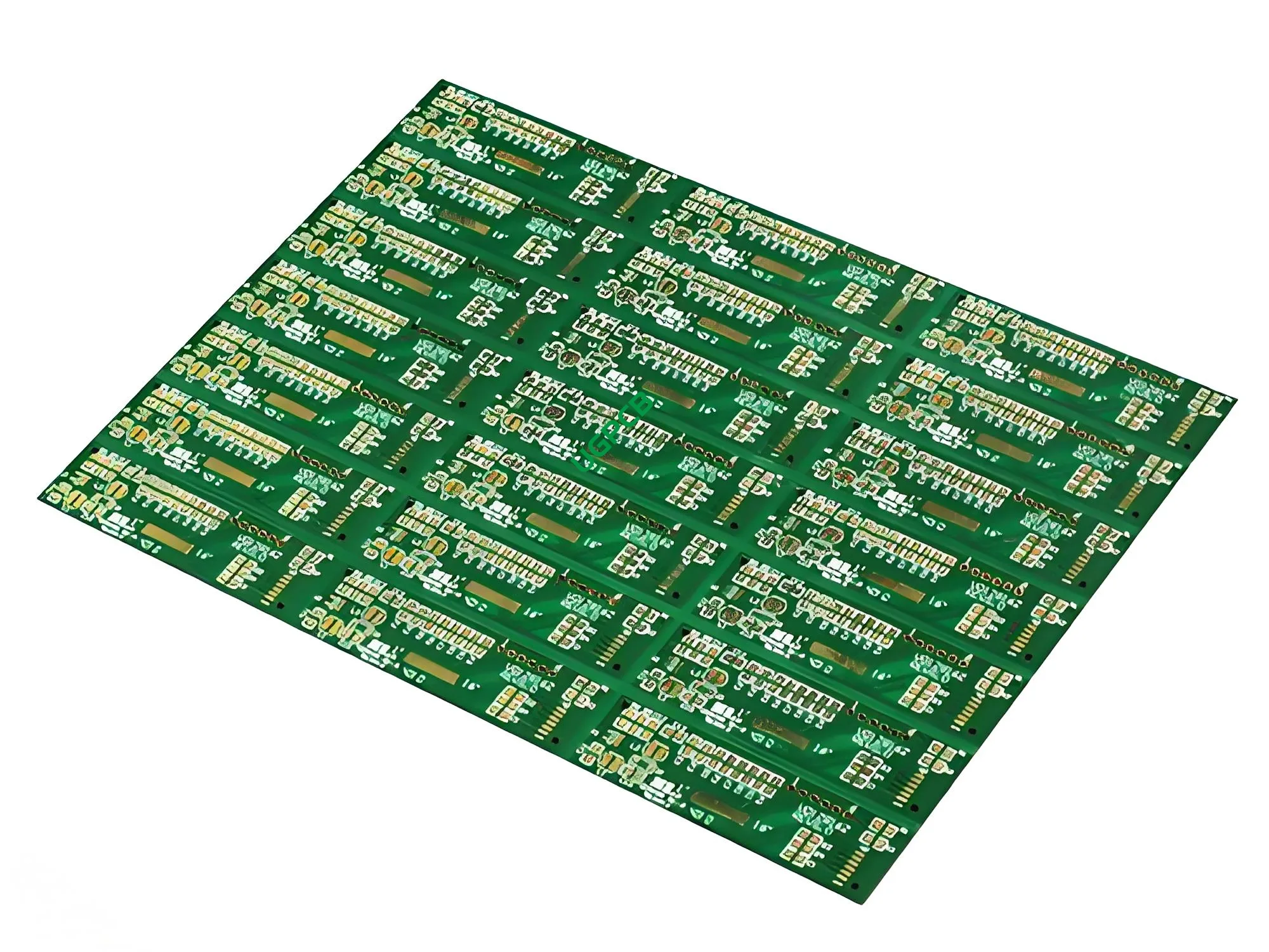
P2.9 LEDプリント回路基板の概要
P2.9 LEDプリント回路基板 (プリント基板) 特別なものです プリント基板 P2.9 LEDモジュールで使用するために設計されています, これは、高解像度ディスプレイアプリケーションで一般的に使用されています. このPCBは、大規模な作成に最適です, シームレスなLEDディスプレイ.
P2.9 LEDプリント回路基板とは何ですか?
p2.9 LEDプリント回路基板はaです プリント基板 (プリント基板) P2.9 LEDモジュールに対応して接続するように特別に設計されています. 用語 “p2.9” LEDモジュールのピクセルピッチを指します, どの測定 2.9 各ピクセル間のミリメートル. このPCBは、LEDモジュールを効率的に相互接続できることを保証します, 電子コンポーネントに安定したプラットフォームを提供します.
設計要件
P2.9 LEDプリント回路基板の設計要件は、そのパフォーマンスと信頼性を確保するために厳しいものです:
- 材料: SY1000-2 TG170 FR4, 優れた電気および熱特性のために選択されます.
- レイヤー数: 6 必要な回路と信号の完全性に対応するためのレイヤー.
- 色: 容易な識別と審美的な魅力のための黒/白.
- 仕上がり厚さ: 1.0構造的完全性と耐久性を提供するMM.
- 銅の厚さ: 1適切な導電率と熱散逸を確保するためのOZ.
- 表面処理: はんだき性と腐食抵抗を高めるための浸漬金.
- 最小トレースとスペース: 4ミル(0.1mm) 細かい回路パターンをサポートします.
- 特性: P2.9 LEDモジュールの密なレイアウトに対応するための小さな間隔のあるパッドを増やします.
それはどのように機能しますか?
P2.9 LEDプリント回路基板は、さまざまな電子コンポーネントが導電性経路を介して相互接続するためのプラットフォームを提供することにより機能します. これらの経路, またはトレース, 銅で作られており、ボードにエッチングされています. SY1000-2 TG170 FR4材料は、PCBがLEDディスプレイアプリケーションの要求に耐えることができることを保証します, 浸漬金表面処理は、これらの痕跡が導電性と耐性のままであることを保証しますが.
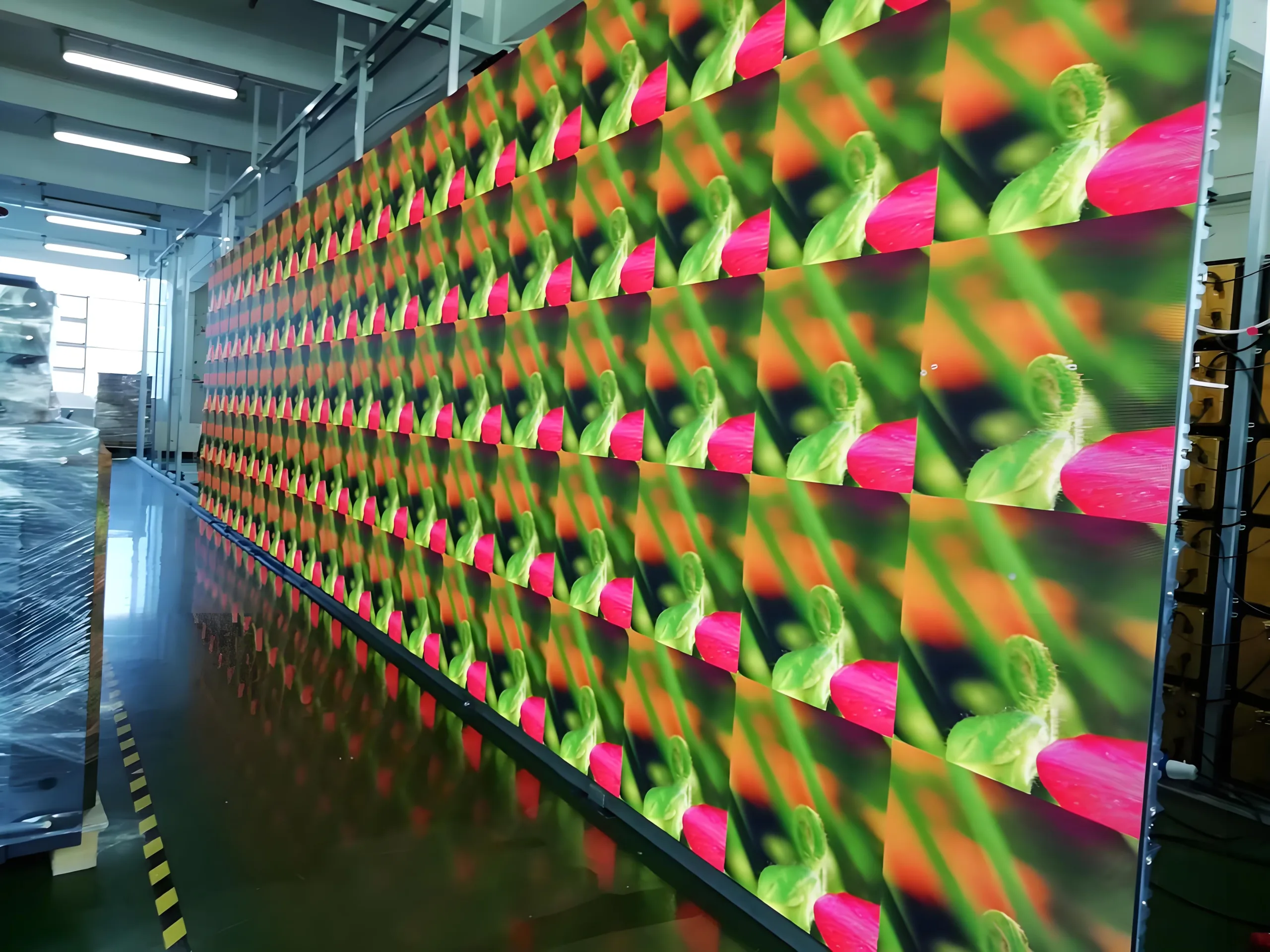
アプリケーション
P2.9 LEDプリント回路基板の主要な適用は、電気信号の流れを管理および調整する高解像度LEDディスプレイシステムにあります. これには含まれます:
- 屋内および屋外LEDディスプレイ
- デジタルサイネージ
- 大きなフォーマットビデオ壁
- イベントステージとコンサート画面
分類
その機能とアプリケーションに基づいています, P2.9 LEDプリント回路基板は、高密度として分類できます, 高速デジタルPCB LEDディスプレイアプリケーション用に設計されています. この分類は、高周波信号を処理し、安定した電気接続を提供する能力を強調しています.
材料構成
コア 材料 P2.9 LEDプリント回路基板で使用されるのはSY1000-2 TG170 FR4です, 優れた機械式で知られている高性能複合材料, サーマル, および電気的特性. この資料は、PCBがLEDディスプレイアプリケーションの要求に耐えることができることを保証します.
性能特性
P2.9 LEDプリント回路基板のパフォーマンス特性には:
- 高い信号の完全性
- 低信号損失
- 優れた熱管理
- 堅牢な機械的強度
- 長期的な安定性
構造の詳細
P2.9 LEDプリント回路基板の構造の詳細は次のとおりです:
- レイヤー数: 6 レイヤー
- 仕上がり厚さ: 1.0mm
- 銅の厚さ: 1オズ
- 表面処理: イマージョンゴールド
- 最小トレースとスペース: 4ミル(0.1mm)
- 特性: P2.9 LEDモジュールの密なレイアウトに対応するための小さな間隔のあるパッドを増やします.
特徴と利点
P2.9 LEDプリント回路基板の主要な機能と利点には:
- 高密度相互接続性
- 優れた信号の完全性
- 堅牢な機械構造
- 信頼できる長期パフォーマンス
- 審美的な色のオプション (黒/白)
製造工程
P2.9 LEDプリント回路基板の生産プロセスには、:
- 材料の選択: 高品質のSY1000-2 TG170 FR4材料の選択.
- レイヤースタッキング: 配置 6 精度のあるレイヤー.
- エッチング: 過剰な銅を除去して、目的のトレースパターンを形成します.
- ソルダーマスクの塗布: 銅の痕跡を保護するためにはんだマスク層を適用する.
- メッキ: 浸漬金表面処理の適用.
- 組み立て: 層相互接続にPTHとVIAを組み込む.
- テスト: PCBがすべてのパフォーマンス仕様を満たすようにします.
ユースケース
P2.9 LEDプリント回路基板は、ようなさまざまなシナリオで使用されています:
- 高解像度の屋内および屋外LEDディスプレイ
- デジタルサイネージのインストール
- 大きなビデオ壁を備えたコンサートとイベントステージ
- ダイナミック広告画面を備えた小売環境


