

データ集約・超高速信号伝送の時代へ, プリント基板 (プリント基板) 単なるコンポーネントキャリアをはるかに超えたものです; これはシステムパフォーマンスの限界を定義する重要なアーキテクチャです. 高速ネットワーキングなどの要求の厳しいアプリケーション向け, 人工知能コンピューティング, および高度なテスト機器, 標準の FR-4 材料では不十分. UGPCB は、当社の先進的なソリューションでこのニーズに対応します。 22-多層PCB 上に構築された パナソニック メグトロン-6 R-5775G ラミネート, 高周波の課題に対応するように設計, 低損失, 複雑な相互接続性.
1.UGPCB の 22 層 Megtron-6 高速 PCB 製品の概要 & 意味
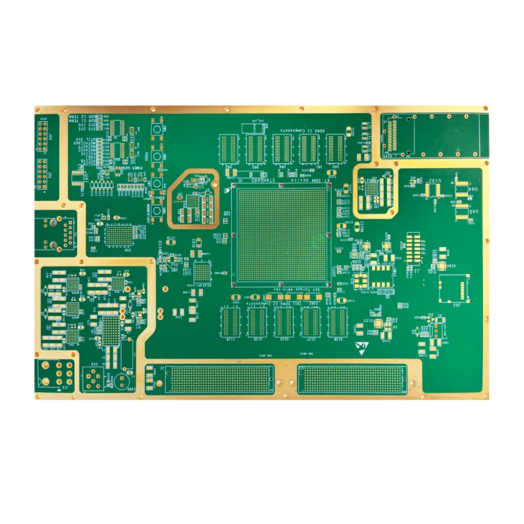
この商品は、 22-層高密度相互接続 (HDI) リジッドプリント基板. その中心的な利点は、プレミアムグレードの使用にあります。, 高速, 低損失ラミネート - パナソニックの Megtron-6 R-5775G. 堅牢な2.0mmの板厚と精密ラミネート技術の組み合わせ, 優れた信号整合性と電力整合性を備えた 10GHz を超える高周波信号を処理できるハイエンドの相互接続プラットフォームを作成します。.

2. 設計上の重要な考慮事項
このような先進的なデザイン 多層回路基板 に集中する必要があります:
-
インピーダンス制御: シングルエンドおよび差動インピーダンスの正確な計算と制御により、Megtron-6 誘電体内での一貫した信号伝播を保証します。.
-
スタックアップ最適化: のインテリジェントな配置 22 導電層 (22レイヤー)—信号を含む, 力, およびグランドプレーンは、シールドを最大化し、クロストークを最小限に抑えるために重要です。 高層数の PCB.
-
熱管理: 2.0mmの板厚と多層構造により熱分散を促進. しかし, サーマルビアの戦略的使用は、高出力 IC 領域にとって引き続き不可欠です.
-
高周波ルーティング: マイクロストリップまたはストリップライン構成の採用, 鋭角旋回を避ける, Megtron-6 の薄型銅箔を利用して表皮効果による損失を低減します。.
3. それがどのように機能するか & 構造
あ PCB の主な機能 絶縁基板上のエッチングされた銅配線を介してコンポーネント間の電気接続と信号伝送を提供します。. これ 22-層PCBボード 構造は精密なものに似ています “多層サンドイッチ”:
-
内層: M/HOZ を使用する (約 1/1 オンスまたは35μm) コア電源用の銅, 地上飛行機, およびいくつかの内部信号ルーティング.
-
外層: 使用 1/1 主要コンポーネントの取り付けと重要な信号トレースの配線にオンスの銅を使用.
-
誘電体層: すべての絶縁プリプレグ材料は、 パナソニック メグトロン-6 R-5775G, 誘電率が低い (DK) および散逸係数 (Df) 優れた高速信号伝送を保証します.
-
表面仕上げ: エレクトロレスニッケルイマージョンゴールド (同意する) で 2 マイクロインチ (2u”). これによりフラットが提供されます, はんだ付け可能な表面, 優れた耐酸化性, 優れたワイヤボンディング能力, 高密度 BGA パッケージおよび RF コネクタに最適.
4. コア素材: パナソニック メグトロン-6 R-5775G
これがこの作品の核心です 先進的なPCB材料. Megtron-6 はパナソニックの次世代製品です, 高速, 低損失基板材料シリーズ.
-
主なパフォーマンス: 極めて低い誘電率を特徴とします (DK~3.5) 超低誘電正接 (Df~0.0015 @ 10GHz), 標準の FR-4 を大幅に上回る性能. 高いガラス転移温度 (TG) 高温リフローはんだ付けプロセス中に優れた熱安定性と寸法の一貫性を保証します.
-
アプリケーションの適合性: 高速デジタル信号に最適化 (10Gbps+ ~ 56/112Gbps) およびミリ波RFアプリケーション.
| アイテム | テスト方法 | 状態 | ユニット | メガトロン6 R-5775(N) 低DKガラス布 |
メガトロン6 R-5775 通常のガラス布 |
|
| ガラス遷移温度。(TG) | DSC | あ | ℃ | 185 | 185 | |
| 熱分解温度。(TD) | TGA | あ | ℃ | 410 | 410 | |
| CTE X軸 | A1 | IPC-TM-650 2.4.24 | あ | ppm/°C | 14-16 | 14-16 |
| CTE Y軸 | 14-16 | 14-16 | ||||
| CTE Z軸 | A1 | IPC-TM-650 2.4.24 | あ | 45 | 45 | |
| A2 | 260 | 260 | ||||
| T288(銅で) | IPC-TM-650 2.4.24.1 | あ | 分 | >120 | >120 | |
| 誘電率(DK) | 12GHz | バランスタイプ 円形ディスク共振器 |
C-24/23/50 | - | 3.4 | 3.6 |
| 散逸係数(Df) | 0.004 | 0.004 | ||||
| 吸収 | IPC-TM-650 2.6.2.1 | D-24/23 | % | 0.14 | 0.14 | |
| 曲げ弾性率 | 埋める | JIS c 6481 | あ | GPA | 18 | 19 |
| 皮の強度* | 1オンス(35μm) | IPC-TM-650 2.4.8 | あ | kn/m | 0.8 | 0.8 |
5. 主な特長 & パフォーマンス
-
超低信号損失: Megtron-6 素材は、最小限の減衰で高周波信号伝送の最大効率を保証します。.
-
優れた保温性 & 寸法安定性: 高いTg値と2.0mm厚の板厚で高温対応, ハイパワーアプリケーション環境.
-
高密度相互接続機能: 22 層設計により豊富なルーティング チャネルが提供されます。, 大規模チップの複雑な相互接続をサポート (例えば。, FPGA, GPU).
-
正確なインピーダンス & レイヤー間の登録: 成熟した製造プロセスにより、製品全体で一貫した電気的性能が保証されます。 多層PCB.
-
優れたはんだ付け性 & ボンディング: 2u” ENIG 仕上げにより信頼性の高いはんだ接合が保証され、精密な SMT アセンブリに適しています.
6. 科学的分類 & 主要なアプリケーション
-
科学的分類:
-
レイヤーカウントごとに: 高多層基板 (通常 >10 レイヤー).
-
素材によって: 高速PCB / 高周波PCB / 低損失PCB.
-
テクノロジーによって: HDI PCB (ブラインド/埋め込みビアなどの特定の設計機能の影響を受ける).
-
剛性別: リジッドPCB.
-
-
主要なアプリケーション & ユースケース:
-
高速ネットワーク機器: 400G/800G 光モジュール用のコア バックプレーンとマザーボード, ハイエンドルーター, とスイッチ.
-
高度なコンピューティング & ストレージ: AIサーバーボード, 高性能コンピューティング (HPC) クラスター, エンタープライズSSDコントローラーボード.
-
航空宇宙 & レーダーシステム: アビオニクス通信およびフェーズドアレイレーダーシステム用のRFフロントエンドおよび信号処理ユニット.
-
上級テスト & 測定器: 高速オシロスコープ内のメインボード, スペクトラムアナライザ, および信号発生器.
-
7. 生産の流れの概要
UGPCB は厳しい基準を順守します。 プリント基板の製造工程 品質を確保するために:
材料切断 → 内層イメージング → ラミネート (22-レイヤーの配置 & ボンディング) → 穴あけ → ホールメタライゼーション → 外層イメージング → パターンメッキ → エッチング → はんだマスク塗布 → ENIG 表面仕上げ → 配線 / 採点 → 電気試験 → 最終検査 (AOL)
あらゆる工程を高精度の設備でサポート, 複数の品質管理チェックポイントが統合されており、 PCB製造プロセス, これを確実にする 22-層 Megtron-6 PCB 設計から納品まで最高の基準を満たします.
ベース素材によって革新的なデザインが制限されないようにする.
次世代通信ハードウェアを開発している場合でも、フロンティア コンピューティングの課題に取り組んでいる場合でも, UGPCB 22-レイヤー高性能PCBソリューション 信頼できるハードウェア基盤は何ですか. 私たちが提供するのは製品だけではありません, ただし、からのフルスペクトルのサポート プリント基板設計のご相談 ラピッドプロトタイピングと量産まで.
クリックして見積もりをリクエストし、専門家の技術文書を受け取ります. 優れたコアでプロジェクトを強化!


