
Professional Definition: What is a 6-Layer High-Frequency Hybrid PCB?
In the fields of 5G communications, 自動車レーダー, and high-end computing, 標準 FR-4 PCBs often fall short in meeting the demands for high-frequency, 高速, and high-stability signal transmission. This is where the 高周波 ハイブリッドPCB becomes critical.
A 6-layer high-frequency hybrid PCB is a multilayer circuit board that integrates different performance-grade 高周波ラミネート 材料 (such as Rogers) with standard or specialized materials through precision lamination. これ hybrid construction strategically places materials to optimize electrical, サーマル, and cost performance across different circuit layers. It serves as the core hardware foundation for complex RF microwave circuits and high-speed digital designs.
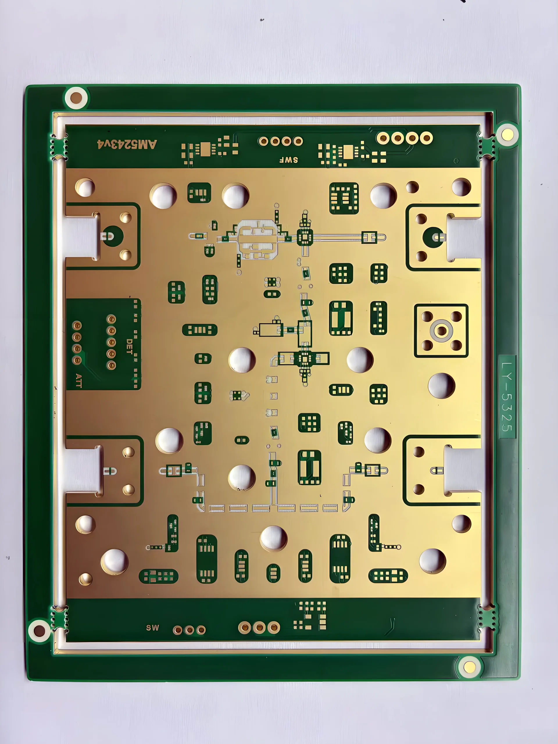

Product Deep Dive: UGPCB’s High-Performance 6-Layer Hybrid Board
1. コア仕様 & 物質科学
-
層 & 工事: 6 レイヤー. This represents an optimal balance between complexity, パフォーマンス, コスト, suitable for integrating digital control and RF front-end circuits.
-
Material Stack-up (Hybrid Core):
Rogers 4350B + Rogers 4450F + IT180A. This is the essence of the design.-
ロジャース4350b: An industry-standard high-frequency circuit board material known for its stable 誘電率 (DK) and low 損失係数 (Df), making it ideal for RF signal layers.
-
Rogers 4450F: A prepreg (PP) with high glass transition temperature (TG) and excellent thermal stability, used for bonding layers and ensuring reliability of the hybrid stack-up under thermal stress.
-
IT180A: A high-performance, mid-loss thermoset material often used for inner signal or power plane layers where good signal integrity is required at a managed cost. This hybrid approach applies the best material where it’s needed most.
-
-
厚さ & 銅の重量: 標準 1.6mm thickness for good mechanical rigidity. Copper weight is
1/H/H/H/H/1 oz, indicating 1 oz copper foil for outer layers そして 0.5 オンス (H oz) copper for inner layers. This facilitates fine-line etching and optimized impedance control. -
表面仕上げ: エレクトロレスニッケルエレクトロレスパラジウムイマージョンゴールド (エネピック): 120 μin Ni, 2 μin Pd, 2 μin Au. This is a premium finish offering excellent solderability, wire-bond capability, および腐食抵抗. It is particularly suited for IC基板 and assemblies requiring multiple reflow cycles or gold wire bonding.
2. 設計上の考慮事項 & 動作原理
-
設計上の考慮事項:
-
インピーダンス制御 & 信号の完全性: Utilizing the stable Dk of Rogers materials, combined with precise stack-up design and trace width/spacing control, enables tight PCB impedance control (例えば。, 50Ω シングルエンド, 100Ω差動), それはにとって重要です high-speed PCB signal integrity.
-
Stack-up Planning: High-speed RF traces are typically routed on the Rogers material layers, while power, 地面, and lower-frequency digital signals are placed on IT180A layers. A symmetrical stack-up (as in this design) helps prevent warpage.
-
熱管理: The superior thermal conductivity of Rogers materials, combined with strategic ground vias and thermal relief designs, aids in dissipating heat from high-power RF components.
-
-
動作原理: This PCB acts as the “skeleton” and “highway system” of an electronic device. Its core function is to mount and interconnect components (RF chips, CPU, コンデンサ, 等). High-frequency signals travel via 電子レンジ用PCB transmission lines on the Rogers layers with minimal loss and distortion; power is distributed stably through inner-layer copper planes; and complex interconnections are achieved via blind and buried vias, shortening paths and enhancing electrical performance.
3. Four Advanced Processes: Ensuring Reliability & パフォーマンス
-
コアのブラインド/埋め込みビア: These vias connect adjacent layers within a core (例えば。, Rogers laminate) without penetrating the entire board. This significantly increases routing density in 高密度相互接続 (HDI) プリント基板, reduces parasitic effects, and improves high-frequency performance.
-
Resin Filled Vias: After plating, through-holes or blind/buried vias are filled with epoxy resin. This prevents chemical entrapment, provides a flat surface for fine-line patterning of subsequent layers, and enhances via reliability.
-
ヴィアインパッド (VIP): A via is placed directly within a component pad, then filled and planarized with resin and copper. This is a hallmark of 高度な HDI PCB, enabling further miniaturization and higher component density.
-
Metalized Edge (Edge Plating): A continuous metal layer (typically copper) is plated along the board edge. This provides excellent EMI shielding, protects internal circuits, and strengthens the edge for connector mating and mechanical wear.
4. Key Performance Characteristics
-
Superior High-Frequency Performance: 低損失, stable Dk for pristine signal transmission in RF PCB.
-
優れた信号の完全性: Precision impedance control meets 高速PCB設計 要件.
-
高密度相互接続 (HDI): Blind/buried vias and VIP technology support 高密度PCB レイアウト.
-
信頼性の向上: Robust hybrid construction, ENEPIG finish, and metalized edges suit demanding environments.
-
Improved Thermal & Shielding Performance: Good thermal conductivity and effective EMI suppression.
5. 科学的分類
-
レイヤーカウントごとに: 多層プリント基板
-
材料の種類別: ハイブリッド / Mixed Material PCB
-
テクノロジーによって: Advanced HDI PCB
-
アプリケーションによって: RF Microwave PCB / High-Speed Digital PCB
6. Standard Production Flow
Engineering Design → Material Prep & Shearing → Rogers Material Laser Drilling (ブラインドバイアス) →デスミア & Metallization → Inner Layer Imaging & Etching → Core Lamination (Hybrid Bonding) → Mechanical Drilling → 樹脂充填 & Curing → Outer Layer Imaging → ENEPIG Surface Finish → Metalized Edge Plating → Solder Mask & Silkscreen → Electrical Test & 最終検査.
7. 主要なアプリケーション (ユースケース)
This product is ideal for high-reliability electronic projects with stringent demands:
-
5G通信インフラストラクチャ: RF PCB within AAUs (Active Antenna Units) and remote radio units.
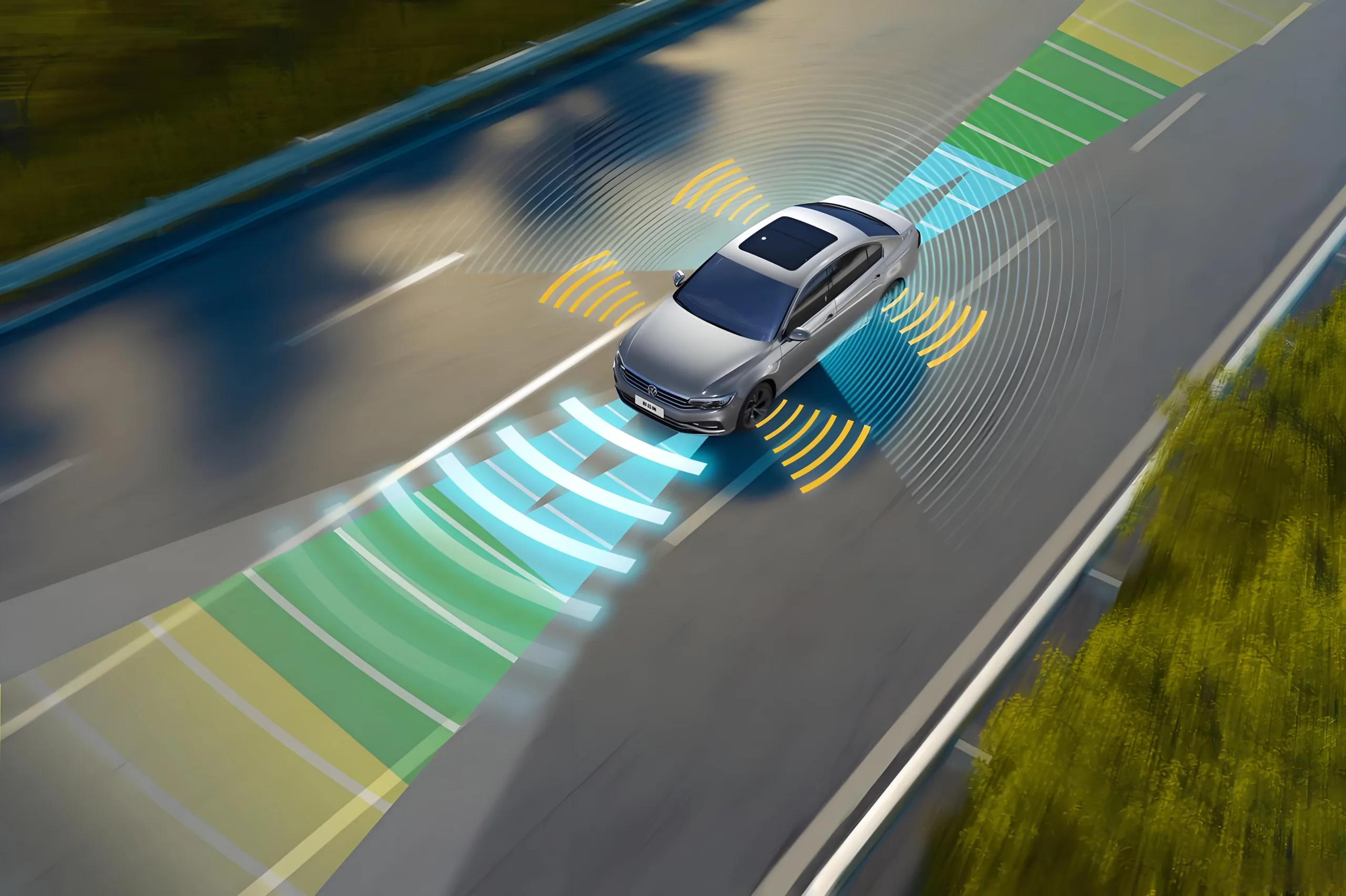
-
カーエレクトロニクス: Radar PCBs for ADAS and autonomous vehicles (例えば。, 77GHz radar).
-
航空宇宙 & 防衛: High-Reliability PCBs in radar systems, satellite comms, and EW equipment.
-
ハイエンドテスト & 測定: Core boards for network analyzers and spectrum analyzers.
-
高性能コンピューティング & データセンター: Backplanes or motherboards for high-speed servers/switches.

Why Choose UGPCB for Your 6-Layer High-Frequency Hybrid PCB?
In advanced プリント基板の製造, consistency and attention to detail determine success. UGPCB possesses deep expertise across the entire complex process chain—from Rogers material processing そして レーザー穴あけ に resin filling そして ENEPIG plating. We deliver not just boards that meet specifications, but robust PCB solutions that ensure your product’s successful volume production.
今すぐお問い合わせください for dedicated technical support and a competitive quote for your 5G PCB, automotive radar PCB, または high-frequency module PCB project. Let UGPCB be your trusted partner for 高周波, high-speed PCB fabrication.