

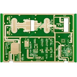
製品の概要
Modern wireless systems face a critical challenge: high-frequency signals demand premium materials, but using Rogers laminates for the entire board drives costs prohibitively high. UGPCB Rogers RO4350B+FR4 High Frequency ハイブリッドPCB solves this dilemma. It combines high-performance RF material with standard FR4 in a single, cost-effective 4-layer stackup .
This hybrid construction places ロジャース RO4350B on the outer layers for critical signal routing. FR4 forms the inner layers for power distribution and mechanical support . The result? Exceptional RF performance at a fraction of the cost of full-Rogers boards .
主な仕様:
-
モデル: ロジャース RO4350B + FR4 High Frequency Hybrid PCB
-
誘電率 (DK): 3.48 @ 10GHz
-
構造: 2 Layers Rogers RO4350B + 2 Layers FR4
-
レイヤー数: 4 レイヤー
-
仕上がり厚さ: 1.6mm
-
Base Copper Thickness: ½ (18μm) HH/HH
-
銅の仕上がり厚さ: 1/0.5/0.5/1 (オズ)
-
表面処理: イマージョンゴールド (同意する)
-
応用: Wireless Induction Communication Systems, RF Front-End Modules
What Is a Rogers RO4350B+FR4 Hybrid PCB?
あ ハイブリッド基板 combines two or more different dielectric materials within a single multilayer board . The Rogers RO4350B+FR4 hybrid uses:
-
ロジャース RO4350B on signal layers: A ceramic-filled hydrocarbon laminate designed for high-frequency applications .
-
FR4 on inner layers: Standard epoxy glass-reinforced laminate for power and ground planes .
This material mix allows engineers to route RF signals on low-loss Rogers material while handling DC power and control logic on cost-effective FR4 .
Advantages at a glance:
-
30-50% コスト削減 compared to full-Rogers boards .
-
Superior signal integrity for high-frequency circuits .
-
機械的安定性 from FR4’s rigid structure .
-
Seamless integration of RF and digital sections on one board .
Design Guidelines and Stackup Structure
レイヤー構成
UGPCB’s standard 4-layer hybrid stackup follows a symmetrical design :
| 層 | 材料 | 銅の重量 | 関数 |
|---|---|---|---|
| L1 (トップ) | ロジャース RO4350B | 1 オズ (finished) | RF signal routing |
| L2 | FR4 | 0.5 オズ (finished) | Ground plane |
| L3 | FR4 | 0.5 オズ (finished) | 力 / low-frequency signals |
| L4 (Bottom) | ロジャース RO4350B | 1 オズ (finished) | RF signal routing |
Total thickness: 1.6mm±10% .
設計上の重要な考慮事項
When designing for this hybrid stackup, follow these rules:
1. インピーダンスマッチング
Rogers RO4350B has Dk=3.48 at 10GHz, while FR4 typically ranges from 4.2-4.8 . This difference affects trace widths for controlled impedance. Always calculate 50Ω or 100Ω traces specifically for the material they reside on.
2. Layer Transition
Keep high-frequency traces entirely within Rogers layers whenever possible . Avoid routing RF signals through FR4 regions to prevent signal degradation.
3. Symmetrical Stackup
The 1.6mm finished thickness with symmetrical copper distribution (1/0.5/0.5/1 オズ) minimizes warpage during lamination .
材料の特性と性能
ロジャース RO4350B
RO4350B belongs to Rogers’ RO4000 series, designed as a direct alternative to PTFE/woven glass materials .
電気的特性 :
-
誘電率 (DK): 3.48 ±0.05 @ 10GHz
-
損失係数 (Df): 0.0037 @ 10GHz
-
熱伝導率: 0.69 w/m・k
熱 & 機械 :
-
ガラス転移温度 (TG): >280℃
-
CTE (z軸): 32 ppm/°C
-
可燃性: UL 94 V-0
RO4350B’s stable Dk across frequency makes it ideal for broadband designs up to millimeter-wave frequencies .
FR4
The FR4 inner layers provide structural integrity and cost efficiency.
Typical Properties :
-
誘電率 (DK): 4.3-4.8 @ 1GHz
-
損失係数 (Df): 0.015-0.025
-
熱伝導率: ~0.3 W/m·K
-
TG: 130-180℃ (depending on grade)
コストの利点: FR4 costs approximately 1/5 に 1/3 of Rogers materials .
Hybrid Compatibility
UGPCB selects modified high-performance FR4 grades that pair well with RO4350B. Recommended matching materials include Isola 370HR, TU-872, そして 落ちた 6 for optimal electrical and thermal compatibility .
Key Advantages of UGPCB’s Hybrid Solution
1. Cost-Performance Balance
By using Rogers only where needed, UGPCB’s hybrid boards deliver:
-
Full RF performance on critical layers
-
30-50% material cost savings 対. all-Rogers designs
-
No compromise on signal integrity
2. 優れた信号の完全性
RO4350B’s stable Dk (±0.05) 保証します :
-
Consistent phase response across temperature
-
Minimal insertion loss at high frequencies
-
Reduced signal dispersion in broadband applications
3. Mechanical Reliability
FR4 cores add stiffness that pure Rogers laminates lack . Benefits include:
-
Reduced warpage during assembly
-
Higher board rigidity for component mounting
-
Better handling through manufacturing
4. 熱管理
RO4350B’s thermal conductivity (0.69 w/m・k) exceeds FR4 by over 2x . Place high-power components on Rogers areas for:
-
Efficient heat spreading
-
Lower operating temperatures
-
Extended product life
5. 優れたはんだき性
イマージョンゴールド (同意する) surface finish provides :
-
Flat pads for fine-pitch components
-
Oxidation resistance
-
Wire-bondable surfaces when required
Manufacturing Process at UGPCB
Producing hybrid PCBs requires specialized process control . UGPCB follows rigorous procedures:
ステップ 1: 材料の準備
RO4350B and FR4 cores are baked to remove moisture . This prevents delamination during lamination.
ステップ 2: 内層イメージング
L2 and L3 FR4 cores undergo standard PCB processing :
-
Dry film lamination
-
LDI exposure
-
エッチング
-
AOI検査
ステップ 3: Layup and Lamination
Critical for hybrid success :
-
Bondply selection (often RO4450B or compatible prepreg)
-
Precise alignment of cores
-
Optimized temperature profile to accommodate different CTEs
-
Gradual cooling to minimize stress
ステップ 4: 掘削
Special considerations for mixed materials :
-
Carbide drills with optimized speeds/feeds
-
Reduced stack height
-
Aggressive peck drilling cycles
ステップ 5: Desmear and Plating
Plasma desmear removes resin smear from drilled holes . Hybrid boards require extended plasma time compared to standard FR4.
ステップ 6: 外層イメージング
L1 and L4 Rogers layers receive:
-
LDI exposure for fine features
-
Controlled etching for impedance accuracy
ステップ 7: 表面仕上げ
イマージョンゴールド (同意する) applied per specification :
-
Nickel: 100-200 µ”
-
金: 2-5 µ”
ステップ 8: 電気試験
100% electrical testing ensures :
-
Continuity
-
Isolation
-
Impedance verification on critical nets
アプリケーションとユースケース
5G Communication Systems
Base station antennas and RRUs benefit from :
-
Low-loss signal paths
-
Cost-effective large boards
-
Stable performance at mmWave frequencies
自動車レーダー (77GHz)
Collision avoidance systems require :
-
Tight Dk control
-
Excellent thermal stability
-
Reliable hybrid construction
無線インフラストラクチャ
Point-to-point radios, Wi-Fi access points :
-
RF power amplifiers on Rogers layers
-
Control logic on FR4
-
Single-board integration
衛星通信
LEO terminals and ground equipment :
-
Low PIM performance
-
Thermal cycling reliability
-
Compact form factors
IoT and Sensors
Industrial wireless systems :
-
Cost-sensitive production
-
Moderate frequencies (2.4GHz, 5GHz)
-
Mixed-signal requirements

製品分類
By industry standards, UGPCB’s Rogers RO4350B+FR4 hybrid PCB falls into these categories:
| 分類タイプ | カテゴリ |
|---|---|
| 素材によって | Rigid Hybrid (混合誘電体) |
| 周波数別 | RF/Microwave PCB (up to mmWave) |
| レイヤーカウントごとに | 多層プリント基板 (4 レイヤー) |
| アプリケーションによって | RF Front-End / ワイヤレス通信 |
| IPC Standard Compliance | IPC-6012クラス 2 |
Why Choose UGPCB for Your Hybrid PCBs?
UGPCB combines technical expertise with manufacturing excellence:
-
10+ 年 of RF PCB manufacturing experience
-
Specialized hybrid process for Rogers+FR4 combinations
-
Full material traceability and stock availability
-
ISO9001, ISO14001, IAF16949, UL certified facilities
-
エンジニアリングサポート for stackup and impedance design
-
Prototype to production 能力
今すぐお見積りを入手してください
Designing high-frequency circuits is challenging enough. Let UGPCB handle the manufacturing complexity.
Email us your Gerber files: sales@ugpcb.com
必要なもの:
-
Layer stackup details
-
Impedance requirements
-
Quantity and timeline
Our engineers will review your design and respond within 24 hours with:
-
Manufacturing feasibility feedback
-
競争力のある価格設定
-
Lead time options
UGPCB – Your Trusted Partner for High-Frequency Hybrid PCBs


