

TG150 PCB 回路基板 導入: 現代のエレクトロニクスにおける熱の課題に対処する
高速通信では, 自動車, 航空宇宙, および高度な産業用制御, 電子機器はますます過酷な動作環境に直面している. 温度が上昇すると標準症状が発生する可能性があります PCB基板 (例えば。, 標準FR-4) ガラス転移を達成するために, 柔らかくすることにつながる, 変形, そして重大なパフォーマンスの損失, システムの信頼性を危険にさらす. を選択する high-tg プリント基板 これらの要求の厳しいアプリケーションで長期的な安定性を確保するには不可欠です.
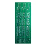
1. 製品の概要: TG150基板とは?
あ TG150基板 です プリント基板 を備えたラミネート材料を使用して製造されています。 ガラス転移温度 (TG) 150℃以上. Tg は PCB 基板の熱耐久性の重要な指標です. 一般的なものと比較して TG130 PCB ラミネート, TG150 材料は、高温下でも優れた物理的剛性と安定した電気特性を維持します。. UGPCB 4-層TG150回路基板 この高機能素材と、 イマージョンゴールド (同意する) 表面仕上げ そしてサポートします 0.08mm細線回路 そして 0.2mmマイクロドリリング, 高信頼性を実現 多層PCB 解決 高度なアプリケーション向け.
2. TG150 PCBのコア材料と強化された性能
-
基本材料: 高性能エポキシまたは改良 FR-4 配合, 一貫して 150°C 以上の Tg を達成するように特別に設計されています。.
-
主なパフォーマンス上の利点 (対. TG130 PCB):
-
優れた熱安定性: Tg が 130°C から 150°C に上昇することで、高温でのボードの変形に対する耐性が大幅に向上します。, 鉛フリーはんだ付けなどの高温の組み立てプロセスに耐える能力を向上させます。.
-
優れた耐湿性と耐薬品性: より緻密な分子構造により、湿気の多い環境での吸湿が軽減されます。, 絶縁抵抗の損失を最小限に抑える (そして) および信号の完全性, 化学物質への曝露に対する優れた耐性を提供しながら.
-
機械的強度と寸法安定性の向上: 高Tg PCB 熱サイクル中に Z 軸膨張係数が低く、より強い接着強度を示します。, 亀裂や層間剥離などのリスクを軽減します.
-
安定した電気的特性: 誘電率 (DK) そして 散逸係数 (Df) 高温の動作温度でもより安定した状態を維持, より高い信号整合性を確保 高周波プリント基板.
-
3. 当社のTG150 PCBの構造と設計仕様
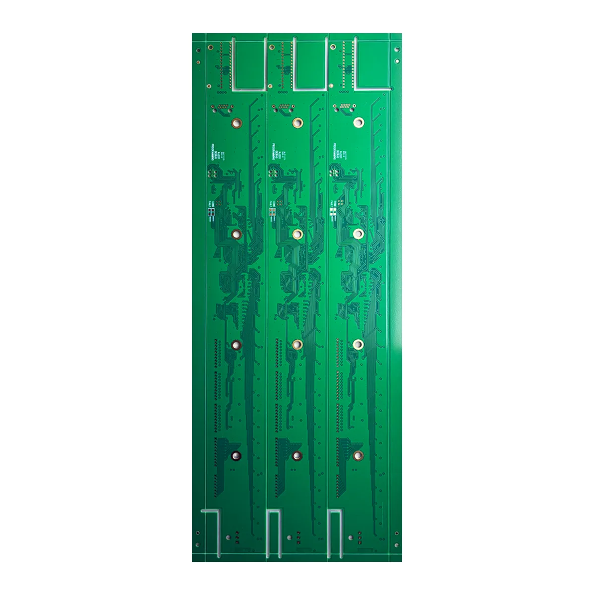
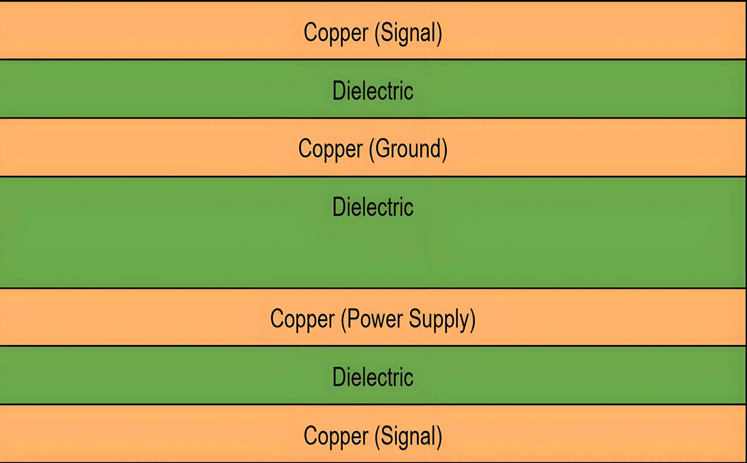
PCB スタックアップ
この商品は標準品です 4-層 PCBボード. 典型的なスタックアップは次のとおりです 信号層 – グラウンドプレーン – パワープレーン – 信号層, 高速信号の完全なリターンパスと効果的なEMI制御を提供します。.
主要な設計機能 & 仕様
最小トレース幅/スペース: 0.08mm / 0.1mm. これは先進的なことを表します 細い線 プリント基板の製造 能力, 高密度ICの配線に不可欠 (例えば。, BGAパッケージ).
ドリル径: 0.2mm. サポート マイクロビアの穴あけ加工, 促進する より高密度の相互接続 基板スペースの節約.
表面仕上げ: イマージョンゴールド (同意する). 平らな表面を提供します, 優れたはんだ付け性, そして長い保存期間, ファインピッチ部品に最適 (例えば。, MF, BGA).
4. 製造工程と品質管理
UGPCB TG150基板製造工程 IPC-6012などの国際規格に厳密に準拠しています (リジッド PCB の認定および性能仕様). プロセスには以下が含まれます:
材料準備 → 内層イメージング → エッチング → ラミネート → 穴あけ (0.2mm) →デスミア & めっき → 外層イメージング → パターンめっき → エッチング → はんだマスク塗布 → ENIG 表面仕上げ → 配線 → 電気試験 → 最終検査.
それぞれの段階で, 先進的な設備を採用しております (例えば。, LDIイメージング, AOI検査) 厳格な信頼性テスト (例えば。, 熱応力, イオン汚染) あらゆる品質を保証するために 高Tg回路基板.

5. 製品分類と代表的な用途
-
技術分類:
-
作者: Tg: 中高 Tg PCB (ガラス転移温度≧150℃).
-
レイヤーカウントごとに: 多層プリント基板 (4-レイヤーボード).
-
テクノロジーによって: 精密基板 (HDI-準備ができている機能).
-
フィニッシュ別: 同意する PCB, 細線PCB.
-
-
理想的なアプリケーション シナリオ:
-
カーエレクトロニクス: エンジンコントロールユニット (カバー), インフォテインメントシステム, 電源管理モジュール – 許容範囲のボンネット内温度が必要.
-
通信機器: 5G基地局PA, 光モジュール, ネットワーク スイッチ – 大電力が持続的に熱を発生する場所.
-
産業用制御: サーボドライブ, plcs, 産業用 PC – 高温の工場環境でも信頼性の高い動作を実現.
-
パワーエレクトロニクス: 高出力スイッチモード電源 (SMPS), インバータ – パワーコンポーネントが大量の熱を発生する場所.
-
航空宇宙 & 防衛: 信頼性と環境耐性が極めて要求される電子システム.
-
6. TG150 PCB に UGPCB を選択する理由?
-
認定された材料: 検証済みのものを使用しています, 追跡可能 TG150 PCB ラミネート 評判の良いサプライヤーからの.
-
精密製造: 当社の専門知識 多層PCB製造 そして ENIG処理 高い収率を保証します 0.08mmの細線デザイン.
-
保証仕様: すべての技術パラメータ (ガラス転移温度150℃, 0.2mmドリル) データシートに対して厳密に検証されています.
-
エンドツーエンドのサポート: 私たちは完全な技術サポートを提供します プリント基板設計 レビュー そして インピーダンス制御 ラピッドプロトタイピングと量産まで.
7. 行動を起こしてください: 堅牢な基盤で設計を保護
熱制限が製品の革新を妨げないようにする. UGPCB の選択 高信頼性TG150基板 並外れた安定性への投資を意味します, 耐久性, とパフォーマンス.
行動を促す
*(画像の提案: 通信または自動車アプリケーションで使用される実装済みの TG150 PCB の高品質クローズアップ写真。)*
すべてがかかる: High-density assembled 4-layer TG150 PCB with ENIG finish for automotive or telecom applications
次のプロジェクトは熱信頼性の課題に直面していますか??
厳しい環境ストレスに耐えられる PCB が必要ですか??
今すぐ UGPCB 専門家チームにお問い合わせください!
[TG150 PCB の無料見積もりを取得するにはここをクリックしてください]
[ガーバー ファイルをアップロードして 24 時間のデザイン レビューを実施]
高性能の専門知識を当社にお任せください プリント基板の製造 あなたの成功に力を与える.


