

高速・高周波エレクトロニクスの世界, メッキのあらゆるミクロンと表面の平坦度のあらゆる側面が、信号伝送の純度と最終製品の信頼性を直接決定します。. AIサーバーなどの最先端分野として, 新エネルギー車用エレクトロニクス, と 5G 通信により、ますます厳しいパフォーマンス要求が課せられます。 プリント基板 (プリント基板), 従来の表面仕上げプロセスは限界に直面しています. それに応じて, UGPCB has made a significant investment and officially launched an industry-leading “Fully Automated ENIG (イマージョンゴールド) Post-Processing Line.” This is not merely an equipment upgrade but a solemn commitment to providing comprehensive reliability solutions for high-end プリント基板 (印刷回路基板アセンブリ) 顧客, 基板から完成品まで.
同意プロセス: ハイエンド PCB 製造に必須の選択肢である理由?
各種プリント基板表面仕上げ加工の中から, エレクトロレスニッケルイマージョンゴールド (同意する) 独特の物理的および化学的特性により際立っています. ENIG プロセスは、単に銅の表面を金の層で覆うだけではありません。. これは、最初に銅の表面にバリアとして高密度のニッケル - リン合金層を化学堆積する複合プロセスです。, 続いて、ニッケル層上に高純度の金層を置換蒸着します。.
高周波用, 高速PCB製造と 高密度相互接続 (HDI) ボード, ENIG の利点は何にも代えがたいものです:
-
優れた信号の完全性: ENIG はパッドのみを正確にカバーします, 銅層を主な信号伝送媒体として残す. This effectively avoids “skin effect” losses in high-frequency signal transmission, これはミリ波レーダー ボードと GPU インターコネクト ボードにとって重要です.
-
優れた表面の平坦性: 金層が均一な厚さで堆積します, BGA や QFN などのファインピッチ コンポーネントの SMT アセンブリにほぼ完璧な平坦な表面を提供します, はんだボイドやトゥームストンなどの欠陥を大幅に軽減します.
-
延長された保存寿命とはんだ付け性: ENIG ボードは酸化に強い, 保存期限を超えるもの 12 数か月 - HASL よりもはるかに長い (3-6 月) およびOSPプロセス. これにより、コンポーネントの調達と生産スケジュールに大きな柔軟性がもたらされます。.
-
優れた接着性能と接触性能: 高純度の金の表面は、金ワイヤボンディングに理想的なインターフェースを提供し、低電圧を保証します。, ゴールドフィンガーなどのコンポーネントの安定した接触抵抗.
テーブル 1: 主要なプリント基板表面処理工程の比較
| プロセスの種類 | 同意する (イマージョンゴールド) | 出血 (鉛フリー) | OSP (有機はんだ付け性防腐剤) |
|---|---|---|---|
| 平面度 | 素晴らしい, ファインピッチ部品に最適 | 貧しい, prone to “tin whiskers” | 素晴らしい |
| 貯蔵寿命 | >12 月 | 3-6 月 | ~6か月 (厳密な湿度管理が必要) |
| はんだ付け性 | 素晴らしい, 複数回のリフローサイクルでも安定 | 良い | 良い, ただしリフローサイクルは限られている |
| 理想的な用途 | 高周波, HDI, BGA, ゴールドフィンガーズ | 家電, ワイドパッド | 低コスト, ライフサイクルの短い消費者製品 |
| 環境 | 良い (シアン化物を含まないプロセスを使用できる) | 鉛フリーコンプライアンスに対する高い要件 | 素晴らしい |
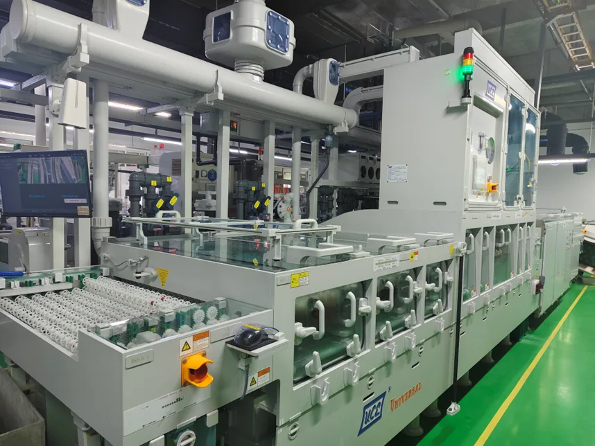
UGPCB の ENIG 後処理ライン: 技術パラメータとプロセスの詳細な分析
UGPCB の新しい ENIG 後処理ラインは、インテリジェントな制御と洗練された管理を特徴とする垂直統合された連続生産ラインです. その設計は標準的な手順を超えています, あらゆる重要な局面で当社のプロセス専門知識と品質への取り組みを組み込む.
1. 前処理: 信頼の接着の基礎
優れたメッキ層はすべて、完璧な銅表面から始まります。. 当社の生産ラインは多段階の精密洗浄とマイクロエッチングシステムを採用しています。. 正確に制御された酸性過硫酸ナトリウム溶液の使用, 銅表面のマイクロエッチングを最適な範囲の0.5~1.5μmに維持します。. このステップは非常に重要です。酸化銅を完全に除去するだけでなく、均一な表面を作成します。, 微細な微細粗さ, その後のニッケル層の緻密な接着のための強固な基盤を築く.
2. アクティベーション & 無電解ニッケル: 堅牢なバリア層の構築
アクティベーションはENIGプロセスの核心です. 高度なパラジウム活性化システムを利用しています. パラジウムイオン濃度を精密に制御することで (20-40 ppm) 温度変動と (±1℃以内), 銅表面への触媒パラジウム核の均一な吸着を保証します。, eliminating the risk of “skip plating” or “leaching.”
その後の無電解ニッケル (で) めっきははんだ接合の信頼性の中心的な決定要因です. 最適化された中リン酸性ENプロセスを採用しています。. 蒸着されたニッケル-リン合金層は微細な結晶化を特徴とします, 低い気孔率, 安定したリン含有量. このバリアは銅と金の間の拡散を効果的に防ぎます。, inhibiting the formation of brittle “black nickel” (ニッケルゴールド金属間化合物) 化合物. これにより、長期間の使用や高温環境にさらされた後でも、はんだ接合部の強度と信頼性が維持されます。.
3. イマージョンゴールド: 最終的な保護面
ゴールドイマージョンステージでは, UGPCBは安定性の高いシアンフリー浸漬ゴールドプロセスを採用, 環境への配慮と性能のベストバランスを実現. 最終表面層として, 金の純度と厚さが重要です. 当社のプロセスにより、金層の純度が次を超えることが保証されます。 99.95%, 厚さは0.05~0.3μmの間で精密に制御されています, 明るいレモンイエロー色を呈する. この薄さ, 緻密な金層は、厚すぎる金層によって引き起こされるはんだ接合部の脆化を防ぎながら、優れた耐酸化性と接触性能を提供します。.
インテリジェントコントロール & 品質保証: ハードウェアを超えた競争力
ハードウェアは骨格です, しかし、インテリジェントなプロセス制御は生産ラインの中枢です. UGPCB の ENIG 後処理ラインの中核となる競争力はここに体現されています:
-
MTO (金属売上高) インテリジェントポカヨケシステム: 特許技術と同様の高度な管理システムを導入しています. コア量産モデルに基づく (例えば。, W = TλNCη のようなパラメータを含む, ここで、Wは金の総重量です, 時間だよ, と λ, C, η は製品/効率に関連するパラメータです) 各バッチの ENIG エリアと数量を組み合わせます, システムはゴールドタンクの実際の MTO 値を自動的に計算します。. 生産前, 実際の値を標準と比較します. 事前に設定された MTO に達するか超過すると, the system “poka-yokes” (間違い防止) バッチロードをロックして禁止することによって. これにより、はんだパッドの不濡れや化学的寿命の消耗による腐食などのリスクが根本的に防止されます。, すべての基板が最適な化学活性範囲内で処理されるようにする.
-
フルプロセスのデジタルパラメータモニタリング: このラインには、リアルタイムのデータ収集と温度の閉ループ制御を実行する中央監視システムが統合されています。, pH, 集中, 各タンクの浸漬時間 (クリーニング, マイクロエッチ, 活性化, ニッケル, 金, 等). すべてのデータは追跡可能です, providing a “data fingerprint” for process stability and quality consistency.
-
最適化された後処理リンス: 高品質のENIG要件に厳密に準拠, 主要工程後に十分な逆流多段階すすぎを設定しています。. 後続のタンクの銅イオン汚染を防ぐために、マイクロエッチング後のすすぎの清浄度には特別な注意が払われます。, パラジウム活性化浴の寿命に影響を与える可能性があります。.
未来に力を与える: UGPCB の ENIG プロセスの業界での応用と取り組み
この高度な ENIG 後処理ラインを活用する, UGPCB はお客様に目に見える価値の向上を提供します:
-
高頻度のアプリケーションの課題を克服する: 車載用ミリ波レーダー基板向けに信号損失を最小限に抑えた表面仕上げソリューションを提供, 5Gアンテナボード, AI サーバー バックプレーン, Rogersのようなハイエンドラミネートのプロセス要件を満たします.
-
超高密度設計をサポート: の組み立て要件を完全にサポートします。 01005 小型コンポーネントと0.2mmファインピッチBGA, ウェアラブルデバイスやハイエンド医療用電子機器のPCBAに最適です。.
-
長期信頼性の確保: 優れた耐酸化性と耐腐食性により、要求の厳しい産業分野で優れた性能を保証します。, 自動車エレクトロニクス, および航空宇宙環境.
-
迅速な応答 & 一貫性: 完全に自動化されたラインにより、非常に高いプロセスの再現性と安定性が保証されます。, からのシームレスな移行をサポート PCBプロトタイプ 製造から PCBAの大量生産, 有利なリードタイムを提供する.
結論
の領域で プリント基板の製造, 精度はミクロン単位で測定されます, the refinement of every process detail represents a responsibility toward our customers’ product reliability. UGPCB の新しい ENIG 後処理ラインの試運転は、ハイエンド PCB 製造および PCBA アセンブリにおける能力の新たな段階への参入を示しています。. 私たちが納品するのは基板だけではありません, ただしパフォーマンスの保証, 信頼性, そして信頼する. 業界パートナーやお客様にぜひお越しいただき、当社のプレミアム PCB 製造および PCBA アセンブリ サービスがどのようにしてお客様の次世代主力製品の成功を守ることができるかについて話し合うことを心からお勧めいたします。.