
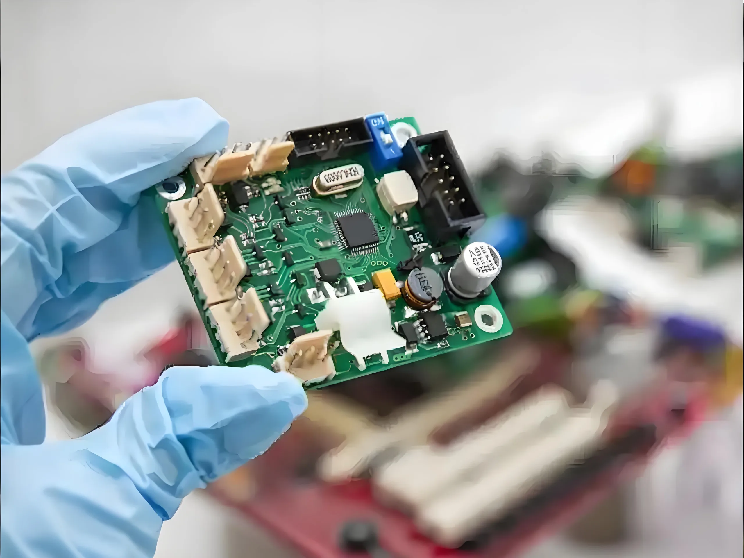
현대 전자 제조에서, 프로세스 결함 PCB (인쇄 회로 보드 어셈블리) 제품 신뢰성을 줄일 수 있습니다, 생산 비용 증가, 그리고 심지어 프로젝트 실패조차도. 통계에 따르면 PCBA 프로세스 결함이 과도하게 설명되어 있습니다 30% 전자 제품의 초기 실패, 솔더 관절 문제와 도금 결함이 1 차 고장 유형입니다.. 이 포괄적 인 안내서는 10 가지 일반적인 프로세스 결함을 체계적으로 분석합니다. PCBA 제조- 거칠기와 구리 입자를 도금하는 것부터 BGA 솔더 조인트 균열에 이르기까지 IPC 표준-준수, 엔지니어가 제품 품질과 신뢰성을 향상시키는 데 도움이되는 전투 테스트 솔루션.

1. 도금 거칠기: 표면 균일 성의 보이지 않는 살인자
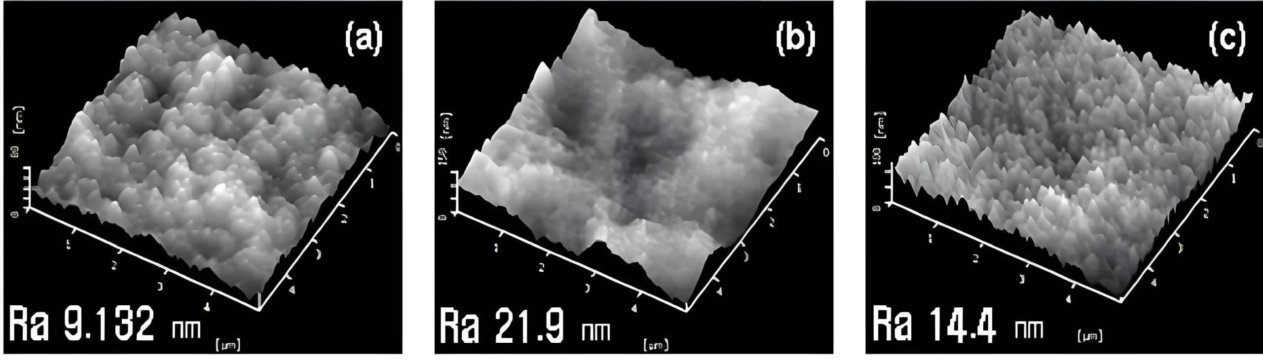
도금 거칠기는 일반적인 결함입니다 PCB 제조, 거친 가장자리 또는 세분화 된 표면 질감이 특징입니다. 가장자리 거칠기는 종종 과도한 전류에서 비롯된 것입니다., 풀 보드 거칠기는 종종 저온 환경에서 불충분 한 밝은 세공 내용 또는 부적절한 재 작업 보드 준비로 인해 발생합니다..

솔루션:
- 도금 매개 변수를 조정하십시오: 안정적인 출력을 위해 전류 밀도를 줄이고 앰 미터를 보정하십시오.
- 첨가사 사용량을 최적화하십시오: 균일 성을 향상시키기 위해 저온에서 브라이트너를 보충하십시오.
- 전처리를 강화하십시오: 오염 물질과 산화물을 제거하기 위해 재 작업 보드를 철저히 청소하십시오.
IPC 표준에 따라, 고품질 PCB 구리 두께 내성을 유지해야합니다. ≤5%. 도금 거칠기가 종종 초과됩니다 10% 편차, 전류 운반 용량에 비판적으로 영향을 미칩니다.
2. PCB 표면의 구리 입자: 프로세스 체인에서의 미세 오염
구리 입자는 보드 표면에 부착 된 구리 곡물로 나타납니다., 알칼리성 탈지수에서 높은 경도와 같은 소스에서 비롯된 것, 필터 시스템 고장, 구리 도금에서 오염 된 활성화 제, 또는 이미지 전송 중에 불완전한 청소.
완화 전략:
- 필터 유지 보수를 향상시킵니다: 필터 요소를 정기적으로 교체하여 목욕 청결을 유지하십시오.
- 세척 시퀀스 최적화: 심포지 후 전송 후 철저한 헹굼 보장 및 패널 저장 시간을 최소화하십시오..
- 목욕 매개 변수를 모니터링하십시오: 구리 함량 및 산도를 제어합니다, 균일 한 분포를 갖는 인산화 된 구리 양극 사용.
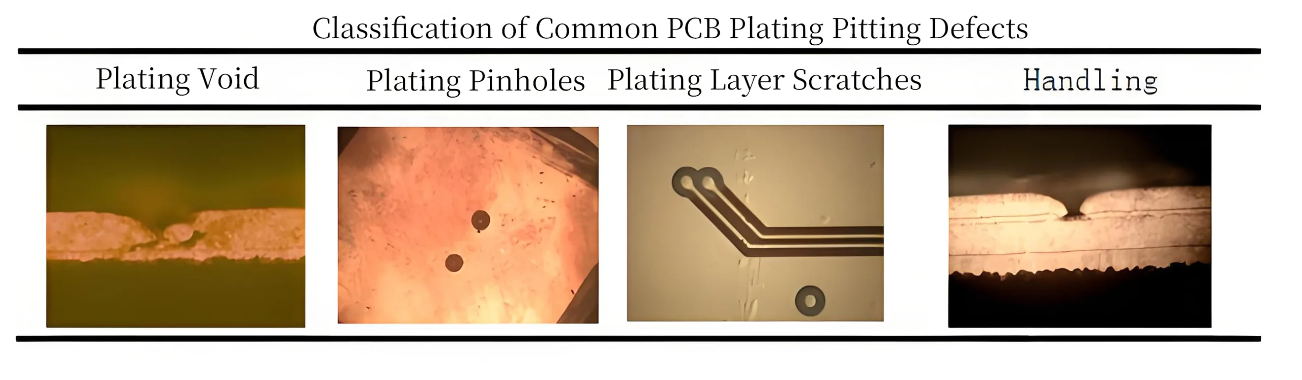
3. 도금 피팅: Spotty 도금의 조용한 살인자
도금 구덩이는 PCB 표면에서 스팟 타이드로 나타납니다, 부적절한 청소에서 오염 된 행거로 인해 발생합니다, 인재되지 않은 이미징 장비, 또는 사전 도금 공정의 경수.

솔루션:
- 구리 도금 행거에 대한 깊은 청소 프로토콜을 구현하십시오.
- 깨끗한 개발을 보장하기 위해 이미징 장비의 정기 유지 보수를 예약하십시오..
- 사전 도금에 탈 이온수를 사용하고 마모 된 행거 코팅을 즉시 교체하십시오..
4. 표면 휘핑 및 색상 불일치: 여러 원인이있는 시각적 결함
표면 휘핑 및 색상 변화는 고르지 않은 공기 교반으로 인해 도금 두께 변화를 일으킨다, 누출 된 필터 펌프, 오염 된면 필터, 불균형 미세-에칭 농도, 빈약 한 수질, 또는 결함이있는 양극 연결.
개선 조치:
- 균일 한 교반을 위해 에어 스파저 위치를 조정하십시오.
- 유기 오염 물질을 제어하기 위해 적격 필터 매체를 교체하십시오.
- 마이크로 에칭 프로세스를 최적화합니다, 수질을 향상시킵니다, 양극 연결을 확인하십시오.
수치: 고성능 현미경 하에서 PCBA 보드의 품질 검사는 도금 거칠기와 구리 입자를 보여줍니다..
5. 통로 장치 납땜 결함: 신뢰성 문제
THD 납땜 결함, ~와 같은 8.7% 산업 제어 보드에서 잘못된 납땜, 세 가지 핵심 문제에서 비롯됩니다:
- 물질적 요인: 유리 섬유 직조 밀도의 변화는 고르지 않은 열 분포를 유발합니다.
- 프로세스 요소: 수동 재 작업 중에 부적절한 온도 프로파일 링.
- 설계 요소: 종횡비 (구멍 직경/핀 직경) IPC 아래 1.5 추천.
최적화 프로토콜:
- 동적 온도 제어: PCB 유리 전이 온도에 따라 납땜 인 철 온도 조정 (Tg).
- 습식 보조제: Use ROL1-rated no-clean flux with “secondary wetting” techniques.
- 프로세스 제어: 3 구역 온도 모니터링 및 재료 추적 성을 구현하십시오.
구현 후, 솔더 충전 속도가 뛰어 들었습니다 68% 에게 93%, 열 사이클링 (-40° C ~ 125 ° C) 통과율에 도달했습니다 100%, 그리고 재 작업 시간이 떨어졌습니다 4.2 에게 1.8 단위당 분.
6. HDI 블라인드 및 패드 고장: 고밀도 신뢰성 위험
HDI 보드 소형 디자인을 위해 블라인드 비아 및 미세한 스태킹을 활용하십시오, 그러나 같은 위험을 소개합니다:
- 신뢰성을 통한 맹인: 오정렬을 방지하려면 레이저 드릴링 공차가 ± 0.02mm 이내에 있어야합니다..
- 구멍 벽의 무효: 전기 구리 도금 중에 pH 불균형 또는 불충분 한 활성화 제.
- 구리 두께가 충분하지 않습니다: IPC는 PTH 벽의 경우 ≥20μm의 의무입니다, 그러나 얇은 영역은 지속됩니다.
솔루션:
- 인라인 레이저 마이크로 미터를 통한 실시간 두께 모니터링 (± 1μm 공차).
- Solder-Flux-Substrate 시스템을위한 호환성 데이터베이스를 구축하십시오.
- 환경 센서를 배포합니다 (온도/습도/voc) 자동 경고 임계 값.
7. 프로세스 에지 결함: 과소 평가 된 연쇄 반응의 공급원
가장자리 결함 (버, 잘못 정렬 된 툴링 홀, 박리) 전체 결함 속도를 높이십시오 10-15%. 업계 평균이 표시됩니다 2.2% 에지 관련 문제의 결함률, 결과를 포함하여:
- 툴링 홀 잘못 정렬 >0.1MM 감소 SMT 배치 정확도는 0.2mm입니다 (기준: 0.1mm).
- 가장자리 박리 약화 구조적 무결성 30% 신호 감쇠 증가 15-20%.
- 솔더 브리지 위험을 초래하고 픽 앤 플레이스 노즐이 손상되는 버.
UGPCB의 전체 론적 제어 시스템:
- 스트레스 해소: 25 ± 1 ° C/50 ± 5% RH의 순응 기질 12 시간.
- 정밀 드릴링: 0.003두께 속도 데이터베이스가있는 MM 계정 기계.
- 완전한 추적 성: 실시간 결함 추적을위한 MES 통합.
이러한 측정은 가장자리 결함 속도를 줄였습니다 <0.1%, 훨씬 아래 2.2% 업계 평균.
수치: 가장자리 결함의 현미경은 SMT 정밀도에 영향을 미치는 툴링 오정렬 및 버를 보여줍니다..
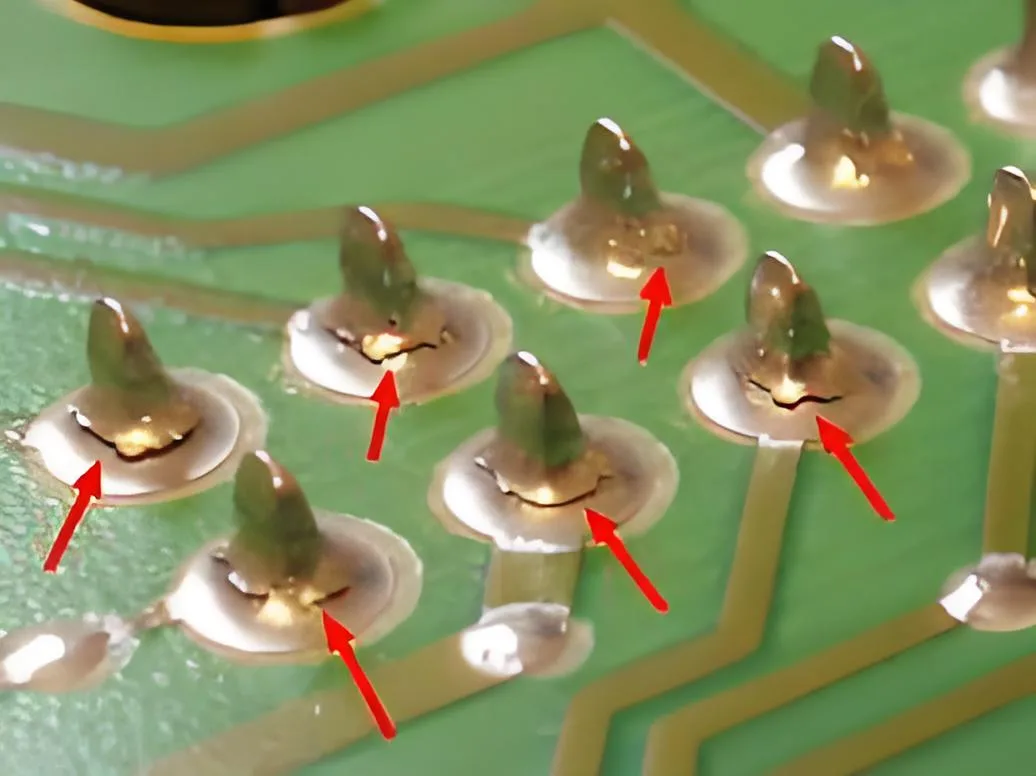
8. 솔더 조인트 균열 및 구성 요소 드롭 아웃: 재료 처리 듀얼 오류
솔더 조인트 균열, 중요한 PCBA 결함, Enig 도금 중에 니켈 층 부식에 종종 추적됩니다. 산화 된 니켈은 솔더로 불균일 한 IMC를 형성합니다, IMC-Nickel 인터페이스에서 균열이 발생합니다.

프로세스 향상:
- 인 제어: 전기 니켈 목욕 수명을 단축하여 인을 증가시킵니다 (높은 P 범위).
- 니켈 두께: 구덩이를 최소화하려면 ≥4μm를 유지하십시오.
- 금 두께: 침수 시간이 감소하여 ≤0.1μm로 제한됩니다.
9. BGA 솔더 조인트 고장: 미세 균열 및 스트레스 농도
BGA 조인트 (0.4MM 피치, 0.2MM 높이) 진동 또는 열 충격에서 미세 균열이 발생하기 쉽습니다. 서버 HDI 사례가 나타났습니다 300% 저항은 진동 시험 후 시험을 증가시킨다.
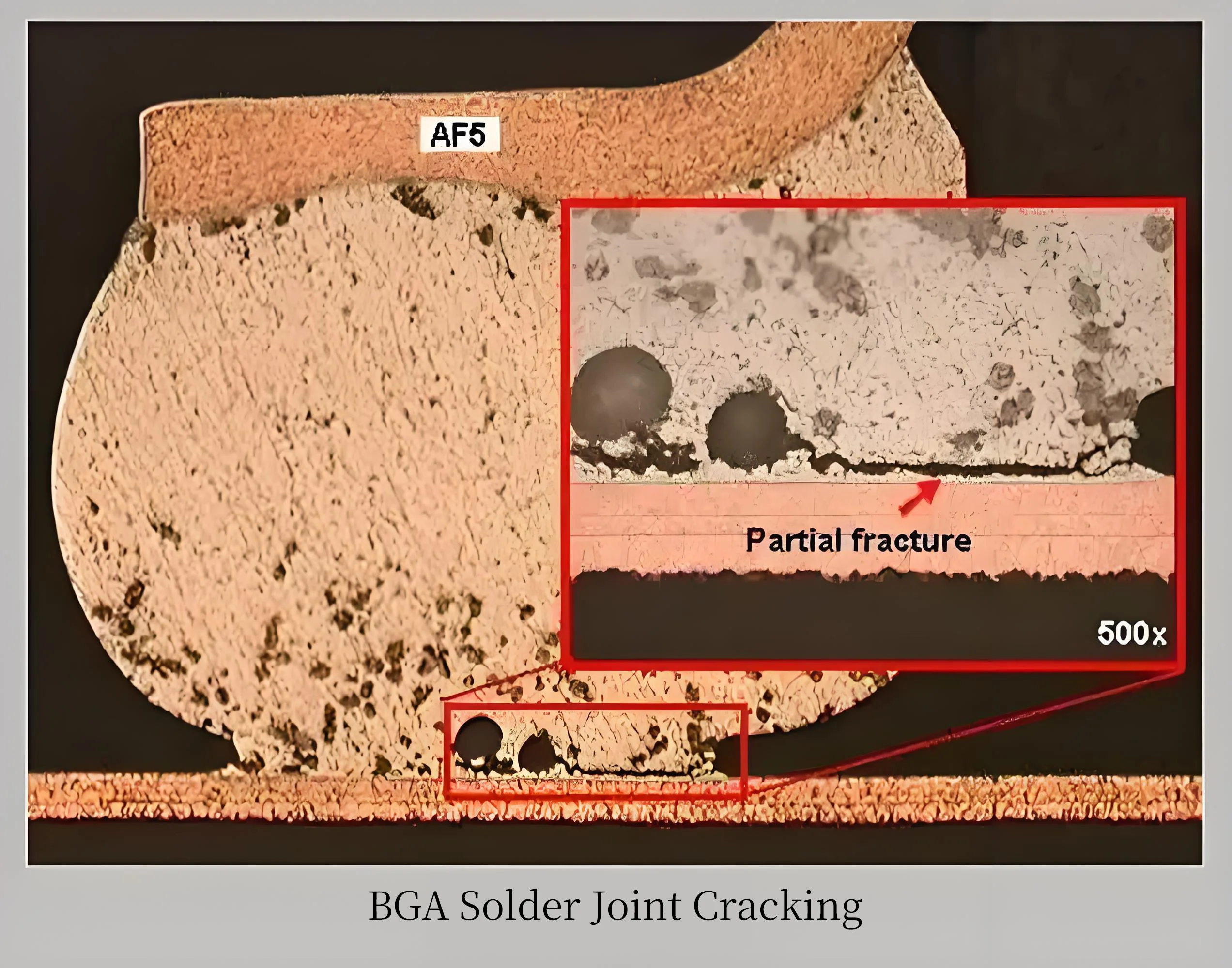

솔루션:
- 레이아웃 최적화: 부적절한 히트 싱크 스크류 배치 강조 BGA를 피하십시오.
- 굽힘 제어: 패드 리프팅을 방지하기 위해 반복적 인 굴곡을 최소화하십시오.
- 재료 일치: CTE와 일치하는 기판/솔더를 선택하십시오 (예를 들어, 8ppm/° C에서 High-TG FR-4. 표준 15ppm/° C).
10. 부적절한 열 설계: 높은 열에서 구성 요소 위기
열 유발 구성 요소 고장이 일반적입니다. A patented “blind-via PCB with integrated heat sink” enhances thermal performance via internal cavities and high-efficiency heat sinks, 열이 빠르게 소산되고 열 손상 위험 감소.
혁신적인 디자인 기능:
- 열공전은 싱크대 열 전달 및 전반적인 냉각을 증가시킵니다.
- 방열판은 PCB 열을 흡수하고 확산시킵니다, 공기 흐름이 효율적으로 열을 전달합니다.
참조를위한 요약 테이블:
| 결함 유형 | 업계 AVG. | 개선 된 비율 | 주요 제어 매개 변수 |
|---|---|---|---|
| 가장자리 결함 | 2.2% | 0.1% | 드릴 정밀도 0.003mm, 12H 적응 |
| 거짓 납땜 | 8.7% | 0.9% | 종횡비 ≥1.5, 3 구역 온도 제어 |
| 구멍 벽 구리 | - | IPC ≥20μm | 두께 내성 ± 1μm |
| 솔더 충전 속도 | 68% | 93% | 동적 프로파일: 280° C/3S + 380° C/2S |

체계적인 프로세스 제어 및 예방은 대부분의 PCBA 결함을 완화 할 수 있습니다.. 숙련 된 공급 업체와 파트너 관계를 맺고 강력한 품질 시스템 구현은 PCBA 신뢰성을 향상시키는 데 중요합니다.. 고출성 PCBA 솔루션 및 기술 상담, 연락하다 오늘 우리.