
에이 회로 기판 종이보다 얇은 것은 이제 글로벌 기술 경쟁에서 중요한 전장입니다.. AI 서버에서 스마트 차량까지, 성능은 전자 제품의 성공 또는 실패를 직접 결정합니다..
UGPCB의 테스트 실험실에서, 엔지니어는 새로 생산 된 AI 서버를 배치합니다 PCB -55 ° C 극심한 추운 환경으로, 그런 다음이 후 125 ° C 고온 챔버로 빠르게 옮깁니다. 30 초. 이 거친주기 테스트는 반복됩니다 1,000 시간-모든 미크론 수준 회로가 극한 조건에서 신호 안정성을 유지하도록합니다..
“Our project nearly missed its deadline due to PCB signal interference!” lamented a tech company R&D 감독. AI 컴퓨팅 붐 및 스마트 차량 전자 건축 혁명으로, 고급 PCB 제조업은 전례없는 기술 혁신 및 용량 경쟁이 진행 중입니다..
01 산업 체인 분석: PCB 제조의 순환 시스템
PCB, hailed as the “Mother of Electronics,” form the core skeleton of nearly all electronic devices. 구성 요소의 기초 플랫폼으로, 그들은 중요한 전기 연결을 가능하게합니다. 그들의 품질은 최종 제품 신뢰성을 직접 결정합니다, 수명, 시장 경쟁력.
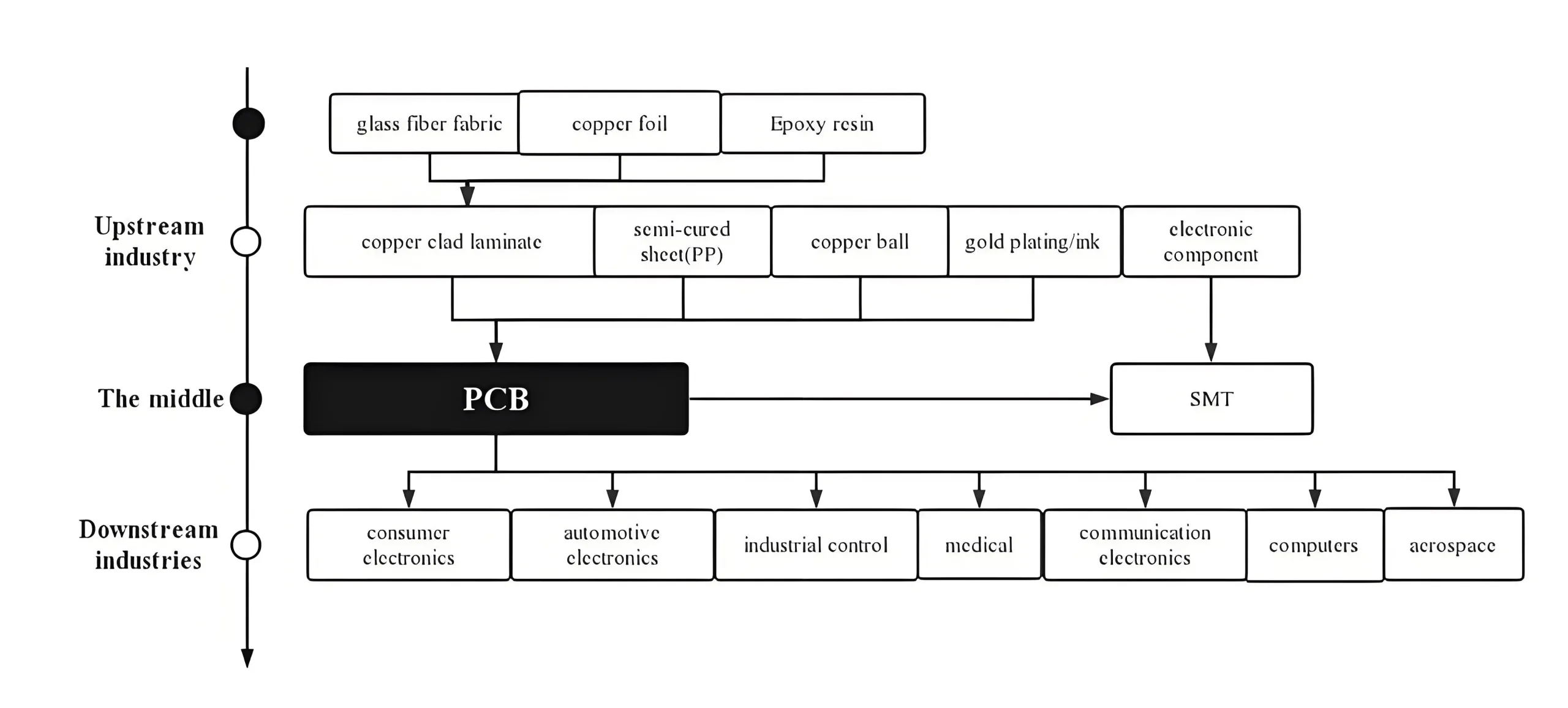

상류: The “Three Kingdoms” Battle in Raw Materials
원자재를 구성합니다 60% PCB 비용의, 구리 클래드 라미네이트 (CCL) 혼자 설명 27.31%. CCL은 구성된 복합재입니다:
-
구리 포일 (42.1% CCL 비용의): AI 서버는 저가성 호일에 대한 급격한 수요를 유도합니다 (순도 ≥99.99%)
-
전자 유리 섬유 직물 (~ 27% 비용): 5G 기지국 & AI 서버에는 저 -DK 유리 직물이 필요합니다
-
합성 수지: 수성 수지 수요가 증가합니다 15% 요, EU Rohs가 운전합니다 & 중국의 에코 스탠드
내의 한복판: PCB 제조의 정밀 엔지니어링
PCB 제조는 예술 및 엔지니어링을 혼합합니다. 최첨단 8 층 3+N+3 HDI 보드 2.5mil/2.5mil을 달성하십시오 (≈0.063mm) 선 너비/간격 정밀도, ± 25μm 이내의 레이저 드릴링 정확도.
핵심 프로세스 혁신:
-
스택 업 최적화: 신호 crosstalk를 줄입니다 30% 임피던스 시뮬레이션을 통해
-
비틀 거리는 미세 비아: 성취하다 15:1 고밀도 라우팅의 종횡비
-
24-시간 노화 테스트: 85 ° C/85% RH 스트레스 하에서 신뢰성을 검증합니다
Prismark 데이터가 표시됩니다 2023-2028 성장: 18+ 레이어 보드 (9% cagr), 중국 HDI (6% cagr, 글로벌 리더), IC 기판 (7% cagr), 유연한 PCB (4% cagr).
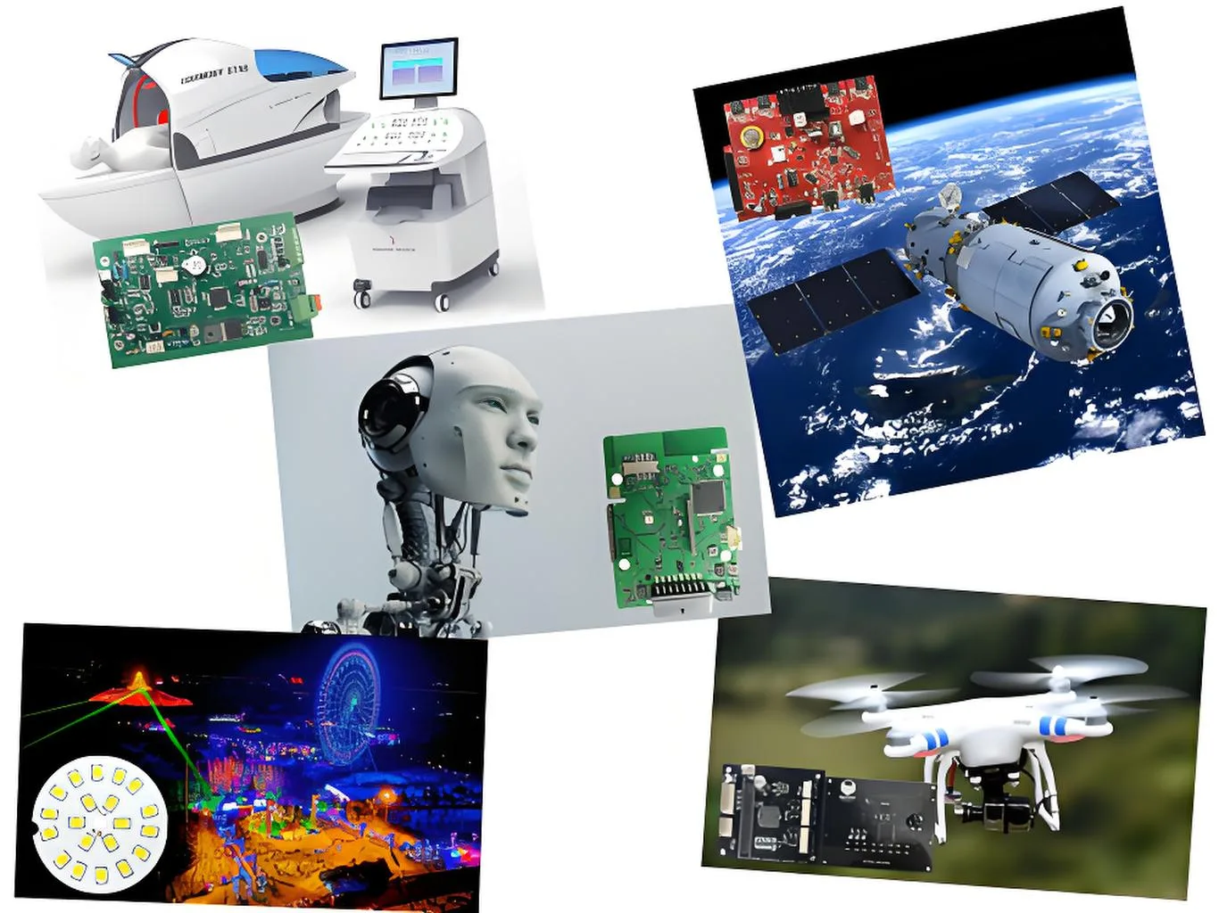
하류: PCB 응용 분야의 폭발성 성장
AI 컴퓨팅 및 스마트 EV는 PCB 수요를 재구성하고 있습니다:
-
AI 서버: 더 높은 PCB 볼륨/가격을 구동하십시오; 랙 당 계산 밀도가 증가합니다 + 엄격한 임피던스 제어 AI 칩
-
새로운 에너지 차량 (NEVS):
-
PCB 컨텐츠 4-5X 전통적인 차량
-
800v 플랫폼이 필요합니다 40% 더 높은 전압 저항
-
ADAS 센서는 고주파 PCB 수요를 향상시킵니다
-
-
의료 전자 장치: 이식 가능한 장치는 이온 오염 ≤1.56μg/cm²를 요구합니다 (NaCl Eq.), 소비자 표준을 훨씬 초과합니다.

02 기술 혁신: 고급 PCB 제조에서 세 가지 중요한 전투
PCB 재료 혁명: 기본 물리에서 양자 효과에 이르기까지
고주파 응용 프로그램에는 새로운 재료가 필요합니다. 5G 기지국은 ± 7% 임피던스 제어가 필요합니다 (>10GHz), 스피어링 소설 수지 r&디:
재료 과학 공식: Df = ε” / ε’
(소산 계수 = 유전체 손실 / 유전율)
낮은 DF/DK 재료는 중추적입니다. 수정 된 PTFE와 같은 업계 벤치 마크 (Df<0.001) 및 탄화수소 수지 (DF = 0.001-0.002) MMWAVE 신호 손실을 오버로 줄입니다 60%.
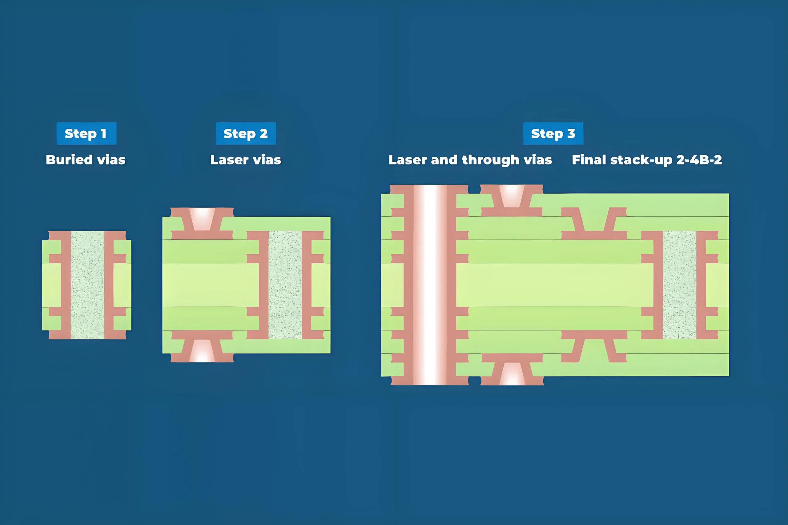
PCB 프로세스 혁신: 미크론 수준 도전
UGPCB의 스마트 공장에서, 레이저 드릴 프로세스 8 층 3+N+3 HDI at 300 구멍/초. 주요 진보:
-
모든 층 상호 연결: 활성화 15:1 종횡비 microvias
-
임피던스 제어: ± 5% 내성 (대. 자동차 레이더의 경우 ± 7%)
-
딱딱한 팩스 기술: 견뎌냅니다 >100,000 굽힘주기
12μm 내의 층 정렬 (1/6 사람의 머리카락) BGA 공동성을 보장합니다 <25% (IPC-A-610 클래스 3), 칩 납땜 실패 방지.

검사 진화: 후반 작업에서 실시간 예측까지
AI-enhanced 자동 X- 선 검사 (axi) BGA 검사 속도 5x를 향상시킵니다, 미스 감소 <0.1%. 고급 고장 분석:
-
육안검사 (100X 현미경)
-
전기 테스트 (네트워크 분석기)
-
X- 선/단면 (SEM/EDS)
-
열 이미징 (핫스팟 탐지)
자동차 등급 PCB에는 -40 ° C ~ 125 ° C 열 순환이 필요합니다 (1,000 사이클) ~와 함께 <0.01% BMS 애플리케이션을위한 임피던스 드리프트.
03 글로벌 경쟁: 용량 이동 & 기술 포지셔닝
지역 역학: 아시아 태평양 지배
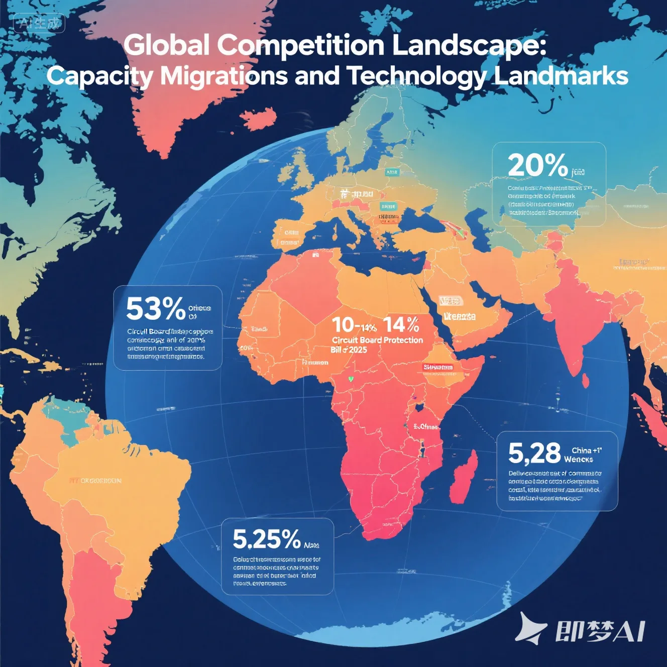
2025 PCB 환경: “East-led, multi-polar growth”:
-
중국: 53% 글로벌 용량 (프리즘)
-
동남아시아: 20% 성장 (태국, 베트남)
-
미국: Subsidies via “Circuit Board Protection Act 2025”
중국의 고급 PCB 상승
중국은 볼륨을 이끌고 있습니다, 출력은 중간에서 낮은 계층으로 유지됩니다 (81% 강성 보드). 주요 기업들은 장벽을 깨뜨리고 있습니다:
-
셰넌 회로: NVIDIA GPU의 FCBGA 기질
-
UGPCB: 자동차 인증 MMWAVE 레이더 PCB
-
Kinwong Electronics: SpaceX 위성 통신 PCB
Research Nester는 Global PCB 시장이 $ 155.38B에 이르렀습니다. 2037, 중국의 고급 점유율이 잠재적으로 증가함에 따라 15% 에게 35%.
04 미래의 전장: 일체 포함 & 전기화 구동 성장
당신은 컴퓨팅이 있습니다: The “Dimensional Leap” for PCBs
AI 인프라 투자는 PCB 기술을 재구성합니다:
-
AI 서버 보드: >20 이제 레이어가 구성됩니다 60%
-
HBM 기판: 선 너비 <8μm
-
광학 모듈 PCB: 80% 저 손실 재료 채택
AI 서버 PCB 시장 CAGR: 16% (서리 & 설리반). AI 전화 사용 30% 더 많은 레이어와 15 FPCS/장치, HDI 채택 가속화.

EV 혁명: Reengineering the Automotive “Heart”
Nev Electronics는 새로운 자동차 PCB 표준을 만듭니다:
-
도메인 컨트롤러: 8-12 레이어 HDI 지배
-
LIDAR 보드: 고주파 PTFE 재료
-
800v 플랫폼: 단열재 견딜 ≥3kv
2025 NEV 판매: ~ 15m 단위. PCB 값/차량 4X 아이스 카. BMS PCB가 필요합니다 0.01% 임피던스 안정성 (-40° C ~ 125 ° C).
지속 가능한 제조: 준수 필수
EU EPR 규정 의무:
-
100% 최대 솔더 2026
-
95% 구리 재활용 속도
-
≥30% 바이오 기반 수지
중국의 배출 기준 수요 40% VOC 감소, PCB 인쇄에서 수성 잉크 채택을 밀어 넣습니다 35% 에게 65% ~에 의해 2027.
05 결론: 전략적 포지셔닝 & 선택
글로벌 PCB 산업은 깊은 변화를 겪고 있습니다. Mordor Intelligence는 84.24B에서 시장 성장을 예측합니다 (2025) $ 106.85b (2030) ~에 4.87% cagr. 주요 기회:
-
고급 용량: 18+ 레이어 보드 (9% cagr), IC 기판 부족 (30%)
-
지역 교대: 25% 동남아시아의 설정 비용이 낮아집니다
-
재료 혁신: 낮은 DK/DF 재료 (40% 요원 수요 성장)

메모: 이 문서에 제시된 데이터는 Prismark를 포함한 권위있는 기관의 최신 보고서에서 제공됩니다., IPC, 그리고 Frost & 설리반. 모든 기술 매개 변수는 CNAS 인증 실험실에서 수행 된 엄격한 테스트를 통해 검증되었습니다.. 프로세스 표준은 IPC-6012EM* 및 IPC-2221B와 같은 현재 에디션 사양을 엄격히 준수합니다..