전문가용 제품 개요
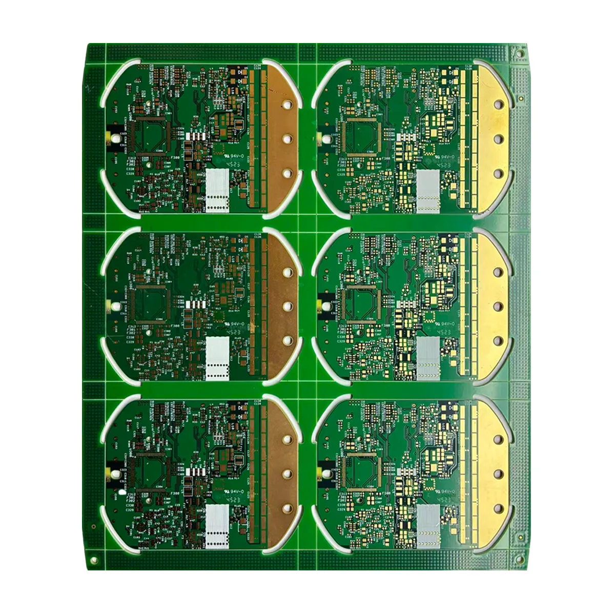
UGPCB 12-Layer Rigid PCB는 고급형 PCB입니다. 다층 회로 기판 복잡한 신호 전송을 위해 설계됨, 고밀도 상호 연결 (HDI), 까다로운 운영 환경. 고성능 FR-4 TU872SLK 라미네이트로 제조되었으며 2-microinch Immersion Gold로 마감되었습니다. (동의하다), 이 보드는 산업 제어 시스템을 위한 초석 솔루션입니다., 통신 인프라, 및 고급 컴퓨팅 하드웨어, 탁월한 전기적 성능 제공, 장기적인 신뢰성, 강력한 신호 무결성.

제품 정의 & 분류
이 제품은 다음으로 분류됩니다. 다층 카운트 리지드 인쇄 회로 기판. 이는 다음과 같이 더 분류될 수 있습니다.:
-
구조 별: 엄격한 PCB.
-
레이어 수에 의해: 12-레이어 다층 보드 (중간에서 높은 레이어 수).
-
기술 별: 복잡한 환경에 적합한 표준 다층 PCB, 극단적이지 않은 소형화 디자인.
-
애플리케이션 클래스별: 산업용/통신 등급 PCB, 높은 신뢰성과 장기적인 안정성에 대한 요구 사항 충족.
중요한 설계 고려 사항
12층 PCB를 설계하려면 세심한 주의가 필요합니다.:
-
스택업 디자인: 합리적인 스택업 시퀀스 (예를 들어, 교대로 신호-접지-신호 레이어) 임피던스 제어에 가장 중요합니다, 누화 감소, 및 전자기 호환성 (EMC). 적절한 12레이어 스택업은 뛰어난 전력 무결성과 신호 차폐를 제공합니다..
-
임피던스 제어: 고속 디지털 신호용 (예를 들어, DDR, PCIE) 또는 RF 라인, 트레이스 특성 임피던스의 정밀한 계산 및 제어 (예를 들어, 50Ω 단일 종단, 90Ω/100Ω 차동) 필수적이다. 우리는 일관성을 보장하기 위해 고급 EDA 도구와 정밀한 프로세스 제어를 활용합니다..
-
힘 & 접지면 관리: 견고한 접지면과 최적화된 전력 분할로 저잡음 전력 공급과 명확한 복귀 경로 보장, 시스템 안정성에 중요한 요소.
-
열 관리: 1.6mm 보드 두께와 FR-4의 열 특성은 구성 요소 전력 손실과 일치해야 합니다.. 고전력 영역에는 열 비아 또는 외부 냉각 솔루션과의 통합이 필요할 수 있습니다..
작동 방식
PCB는 수동적인 플랫폼입니다. 기계적 지원을 제공합니다, 전기적 상호 연결, 신호 전달 경로 전자 부품용. 이 12층 PCB는 칩을 연결하여 완전한 작업 시스템을 용이하게 합니다., 저항기, 커패시터, 등., 에칭된 구리 트레이스의 복잡한 네트워크를 통해. 다층 아키텍처를 사용하면 간섭 없이 서로 다른 레이어에서 트레이스를 교차할 수 있습니다., 회로 복잡성과 통합 밀도가 크게 증가합니다.. ENIG 표면 마감은 안정적인 솔더 조인트와 장기적인 접촉 안정성을 보장합니다..
*(이미지 제안: 12층 PCB 스택업의 상세 단면도)*
*대체 텍스트: 교대로 구리 층과 유전체를 보여주는 12층 PCB 스택의 단면도, 고밀도 인터커넥트를 위한 복잡한 내부 구조를 보여줍니다.*
건설 & 재료
-
레이어 구조: 12 절연 프리프레그로 적층된 전도성 구리층.
-
핵심 자료: FR-4 TU872SLK. 이는 표준 FR-4에 비해 장점을 제공하는 고성능 에폭시 유리 라미네이트입니다.:
-
더 높은 열 안정성 (높은 Tg, 일반적으로 ≥170°C), 열팽창에 대한 더 나은 저항력 제공.
-
우수한 전기적 특성, 안정적인 유전 상수 (DK) 소산 인자 (Df) 고온 및 고주파 조건에서.
-
우수한 CAF (전도성 양극 필라멘트) 저항, 고전압에 이상적, 습도가 높은 환경, 탁월한 신뢰성 보장.
-
-
완성된 두께: 1.60mm (명사 같은), 엄격한 공차 관리로 (일반적으로 ±10%).
-
표면 마감: 무전해 니켈 침지 금 (동의하다). 니켈 두께: 3-5μm; 금 두께: 2 마이크로인치 (대략. 0.05μm). 금층은 니켈이 산화되는 것을 방지합니다., 아파트를 제공하다, 납땜 가능한 표면, 니켈은 구리와 금 사이의 확산 장벽 역할을 하는 반면.
주요 특징 & 성능
-
높은 신뢰성: TU872SLK 고Tg 소재 및 ENIG 마감 처리로 고온에 대한 내성 보장, 부식, 열악한 환경에서 장기간 작동에 대한 적합성.
-
우수한 신호 무결성: 엄격한 스택업 설계와 임피던스 제어로 고속 신호 품질과 낮은 비트 오류율 보장.
-
강력한 내하중 & 열용량: 1.6mm 두께는 견고한 기계적 강도와 상당한 열 부하 관리 기능을 제공합니다..
-
정밀 솔더 플랫폼: The flat 2μ” ENIG surface is ideal for fine-pitch 구성 요소 (예를 들어, BGAS), 그 결과 강한, 결함률이 낮은 안정적인 솔더 조인트.
-
고밀도 상호 연결 (HDI): 12개의 라우팅 레이어가 복잡한 지원, 조밀한 회로 설계, 제품 설치 공간 감소 가능.
제조 공정 흐름
Inner Layer Imaging → AOI Inspection → Lamination & Pressing → Drilling → Electroless Copper Deposition → Outer Layer Imaging → Pattern Plating → Etching → Solder Mask Application → ENIG Surface Finish → Routing & Profiling → Electrical Testing → Final Quality Control (FQC)
응용 & 사용 사례
이 PCB는 안정성과 성능이 중요한 분야에서 널리 사용됩니다.:
-
산업 자동화: PLC 컨트롤러, 서보 드라이브, 산업용 로봇 제어 보드.
-
통신 장비: 라우터, 스위치, 기지국 카드, 광학 모듈.
-
의료 전자 장치: 첨단 의료 영상 시스템용 제어 장치, 환자 모니터.
-
시험 & 측정 장비: 고정밀 오실로스코프, 스펙트럼 분석기, 신호 발생기.
-
힘 & 에너지: 인버터 제어 보드, 배터리 관리 시스템 (BMS) 무대, 스마트 미터.
-
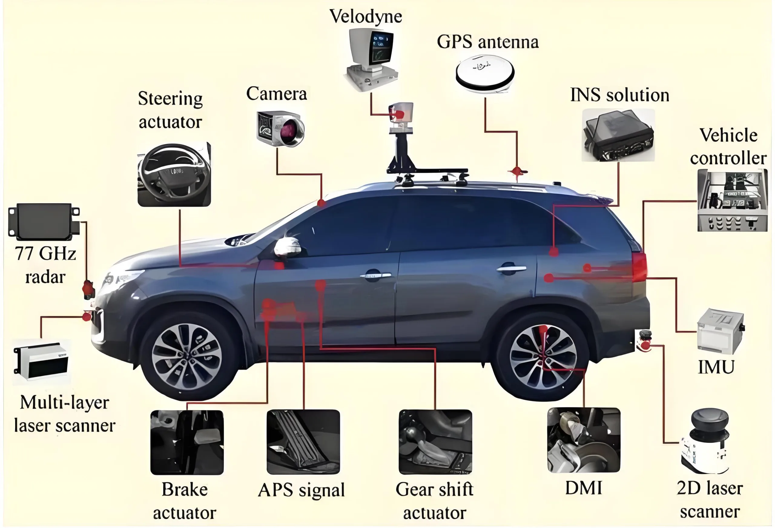
자동차 전자: 고급 인포테인먼트 시스템, 고급 운전자 지원 시스템 (ADAS) 도메인 컨트롤러.