

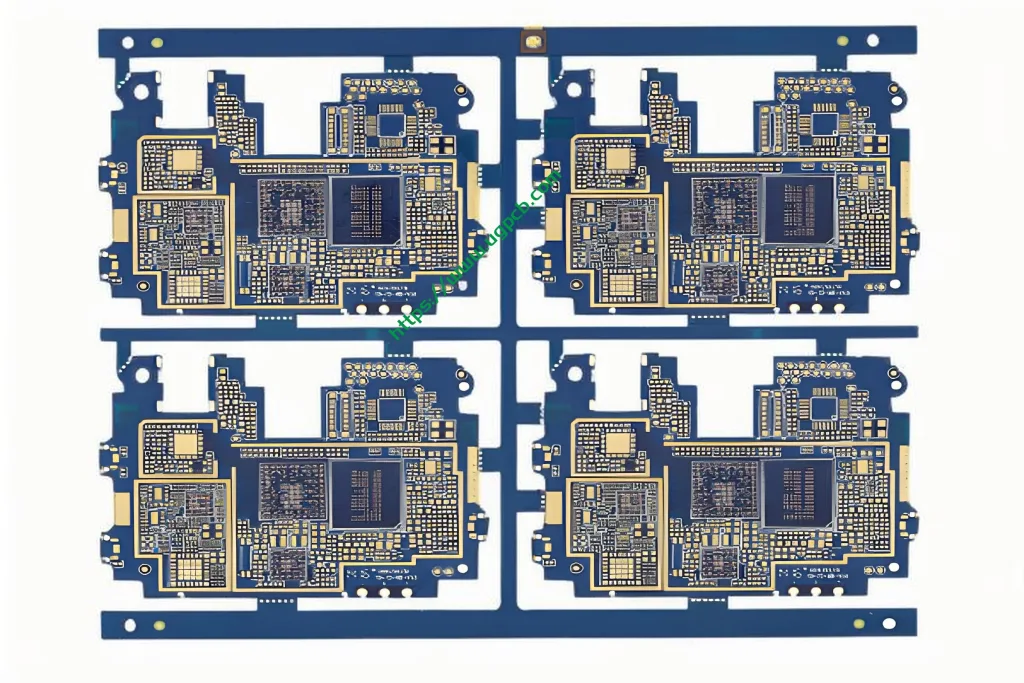
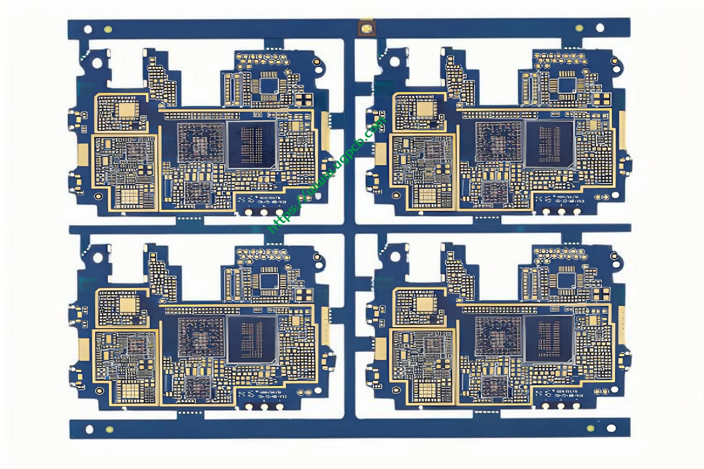
8 레이어 개요 2+N+2 HDI PCB
The 8Layers 2+N+2 HDI PCB is a high – density interconnect 인쇄 회로 기판. 현대 전자 장치에서 중요한 구성 요소입니다, especially those requiring high – precision circuit connections and advanced functionality.

정의
The “8Layers” refers to the number of signal and power/ground layers in the PCB. “2+N+2” is a specific layer configuration pattern. "HDI” stands for High – Density Interconnect, 이 PCB는 밀도의 흔적이 있음을 의미합니다. ( 전도성 경로), 패드, 그리고 vias (층 간의 연결을위한 구멍) per unit area compared to 기존의 PCB.
설계 요구 사항
- 추적과 공간: 최소 추적 및 공간은 3mil/3mil입니다, which requires precise design to ensure there is enough space between adjacent traces to avoid electrical interference and short – circuits.
- 구멍 크기: 구멍 크기에 대한 엄격한 요구 사항이 있습니다. 기계식 구멍은 직경이 0.2mm 이상이어야합니다, 그리고 적어도 0.1mm 레이저 구멍. 이것은 구성 요소의 배치를 수용하고 적절한 전기 연결을 보장하기위한 것입니다..
작동 원리
전기 신호는 PCB의 다른 층의 구리 트레이스를 통해 전송됩니다.. VIAS는 다른 층의 해당 트레이스를 연결합니다, 비교적 작은 공간에서 복잡한 회로를 구현할 수 있습니다.. 전력 및지면 레이어는 전력을 고르게 분배하고 전자기 간섭을 줄이는 데 도움이됩니다..
용도
One of the main applications is in hand – held electronic equipment PCBs. 스마트 폰과 같은 장치에서, 정제, 웨어러블 가젯, 8layers 2+N+2 HDI PCB는 여러 기능을 동시에 처리 할 수 있습니다., 의사 소통과 같은, 처리, 센서 인터페이스, due to its high – density layout.


분류
It can be classified as a multi – layer PCB within the HDI PCB category, 특정 층 아키텍처 8 2+n+2 패턴에 따른 층.
재료
The material used is FR – 4, which is a common fiberglass – reinforced epoxy – laminate material. 그것은 좋은 기계적 강도를 제공합니다, 전기 절연, 그리고 내열성.
성능
- 전기적 성능: 내부 구리 두께가 1oz 및 외부 0.5oz., 전기 신호를 효율적으로 전송할 수 있습니다. 침지 금 표면 처리는 또한 전기 전도성이 우수하며 성분의 납땜 가능성을 향상시키는 데 도움이됩니다..
- 기계적 성능: The FR – 4 재료는 전자 장치에서 정상적인 취급 및 설치를 견딜 수있는 충분한 기계적 안정성을 제공합니다..
구조
그것은 구성됩니다 8 총 레이어. 두 외부 층은 신호 또는 전원/접지 연결에 사용될 수 있습니다., while the “N” layer in the middle can be a flexible combination of signal and power/ground layers according to specific design requirements.
특징
- High – Density: 더 작은 영역에 더 많은 구성 요소를 장착 할 수 있습니다..
- 좋은 표면 처리: 침수 금 처리는 우수한 내식성과 납땜 가능성을 제공합니다.
- 유연한 레이어 구성: 2+n+2 패턴은 다른 회로 설계 요구를 충족하도록 사용자 정의 할 수 있습니다..
생산 과정
- Layer Stack – up: 정리 8 2+n+2 패턴에 따른 층, 적절한 정렬 보장.
- 교련: 설계 요구 사항에 따라 기계식 구멍 및 레이저 구멍을 만듭니다..
- 구리 증착: 구멍과 표면에 구리를 퇴적하여 전도성 경로를 형성합니다..
- 에칭: 과도한 구리를 제거하여 원하는 트레이스 패턴을 만듭니다.
- 표면 처리: 침수 금 처리를 적용하십시오.
- 마무리 손질: Polish and inspect the PCB to ensure it meets the quality standards.

사용 시나리오
앞서 언급했듯이, it is widely used in hand – held electronic equipment. It can also be used in some small – form – factor computing devices or portable medical devices where space is limited but high – quality circuit connections are required.