

6Layer PCB 1+N+1 HDI 개요
6Layers PCB 1+N+1 HDI는 다음과 같은 유형입니다. high – density interconnect printed circuit board. It plays a vital role in various electronic devices where space – saving and high – quality circuit connections are required.

정의
“6Layers” indicates that this PCB 총 6개의 레이어로 구성되어 있습니다. “1+N+1” represents a specific layer configuration, where “1” stands for a signal layer, “N” can be a combination of signal, 힘, 또는 유연한 방식으로 지상층, and the last “1” is also a signal layer. “HDI” means High – Density Interconnect, 이는 단위 면적당 전기 연결 밀도가 높다는 것을 의미합니다..
설계 요구 사항
- 추적과 공간: 최소 트레이스와 공간은 3mil/3mil로 설정됩니다.. 이 엄격한 요구 사항은 정확한 회로 라우팅을 보장하고 인접한 트레이스 간의 전기 간섭 위험을 최소화합니다..
- 구멍 치수: 기계적 구멍은 직경이 0.2mm보다 작아서는 안 됩니다., 레이저 구멍은 최소 0.1mm 이상이어야 합니다.. These dimensions are crucial for proper component mounting and layer – to – layer connections.
작동 원리
전기 신호는 서로 다른 층의 구리 트레이스를 통해 전송됩니다.. 비아는 서로 다른 레이어의 트레이스를 연결하는 데 사용됩니다., 복잡한 회로를 컴팩트한 공간에 구현 가능. 전원 및 접지면은 전력을 균등하게 분배하고 전자기 간섭을 줄이는 데 도움이 됩니다..
용도
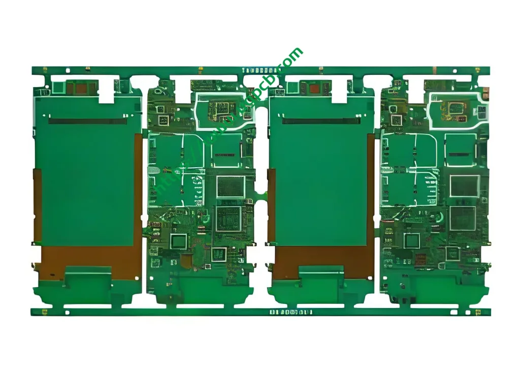
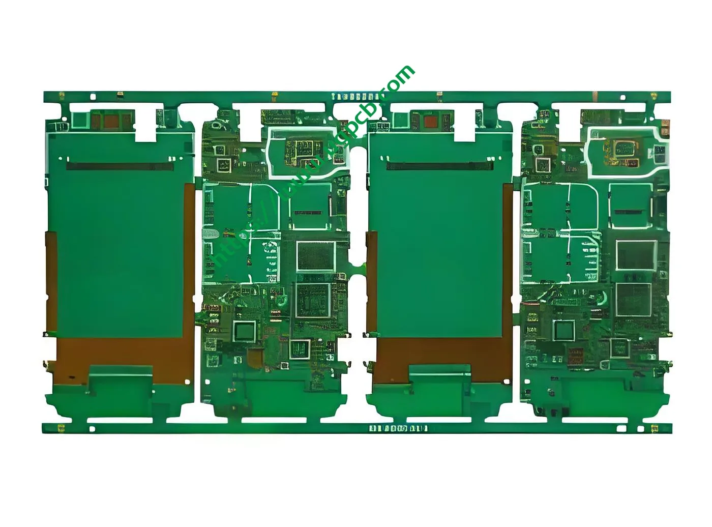
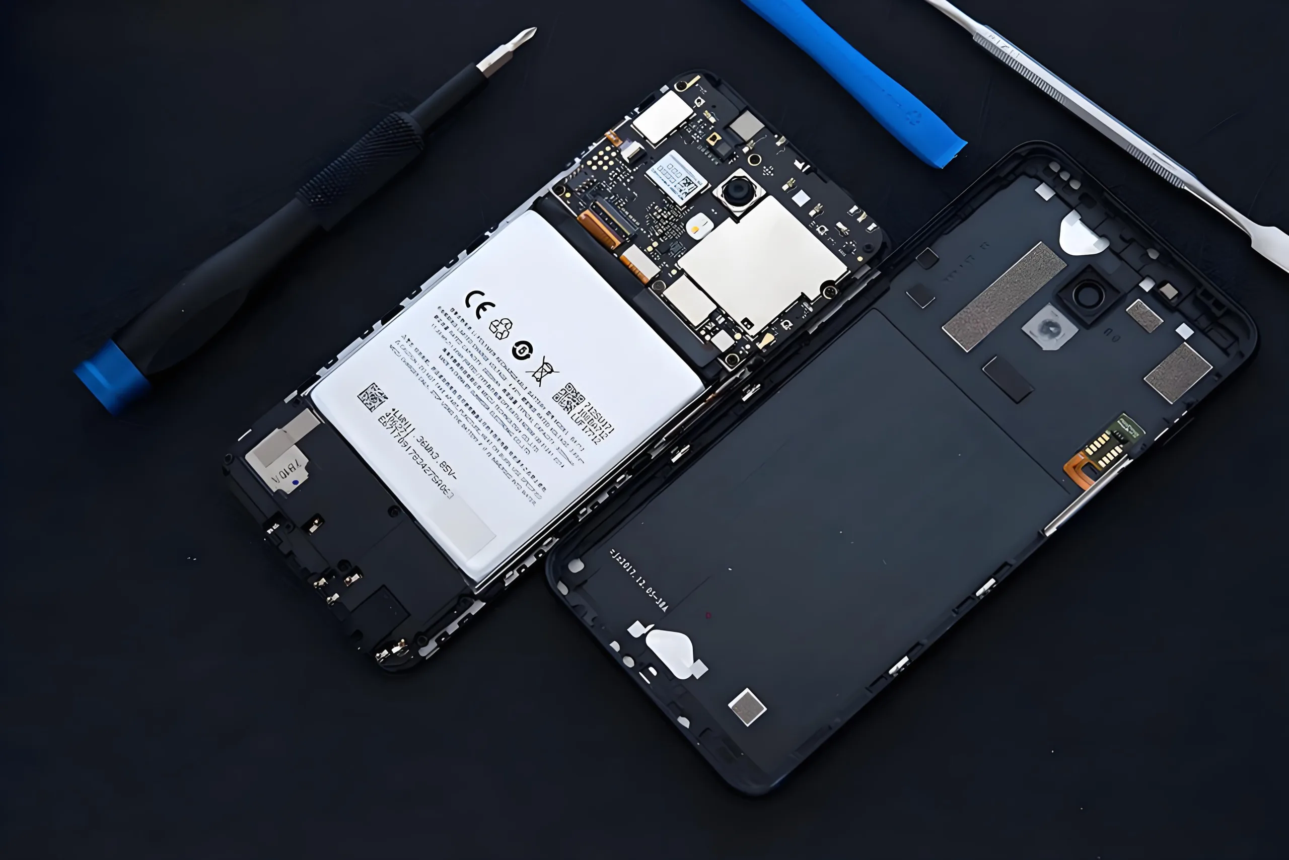
주로 모바일 메인보드 PCB에 사용됩니다.. 휴대폰에서, 이 PCB는 통신과 같은 다양한 기능을 처리할 수 있습니다., 처리, and sensor integration due to its high – density layout.

분류
그것은에 속한다 multi – layer PCB HDI PCB 내의 카테고리. 1+N+1 레이어 구성은 분류의 뚜렷한 특징입니다..
재료
재료는 FR – 4. 이 소재는 우수한 기계적 강도를 제공합니다., 전기 절연, 그리고 내열성, 전자기기의 안정적인 동작을 위해 꼭 필요한.
성능
- 전기적 성능: 내부 구리 두께는 1OZ이고 외부는 0.5OZ입니다., 전기 신호를 효과적으로 전송할 수 있습니다.. 침지 금 표면 처리는 우수한 전기 전도성을 가지며 부품의 우수한 납땜성을 촉진합니다..
- 기계적 성능: The FR – 4 베이스는 모바일 장치의 취급 및 설치를 견딜 수 있을 만큼 충분한 기계적 안정성을 제공합니다..
구조
총 6개의 레이어가 있습니다. 두 개의 외부 레이어는 일반적으로 신호 또는 전원/접지 연결에 사용됩니다., and the “N” layer in the middle can be customized according to the specific circuit design needs.
형질
- 컴팩트한 레이아웃: Due to its high – density design, 더 작은 영역에 더 많은 구성요소를 수용할 수 있습니다..
- 우수한 표면 마감: 침지 금 처리는 내식성과 우수한 납땜성을 제공합니다..
- 유연한 구성: 1+N+1 레이어 배열은 다양한 회로 설계 요구 사항을 충족하도록 조정될 수 있습니다..
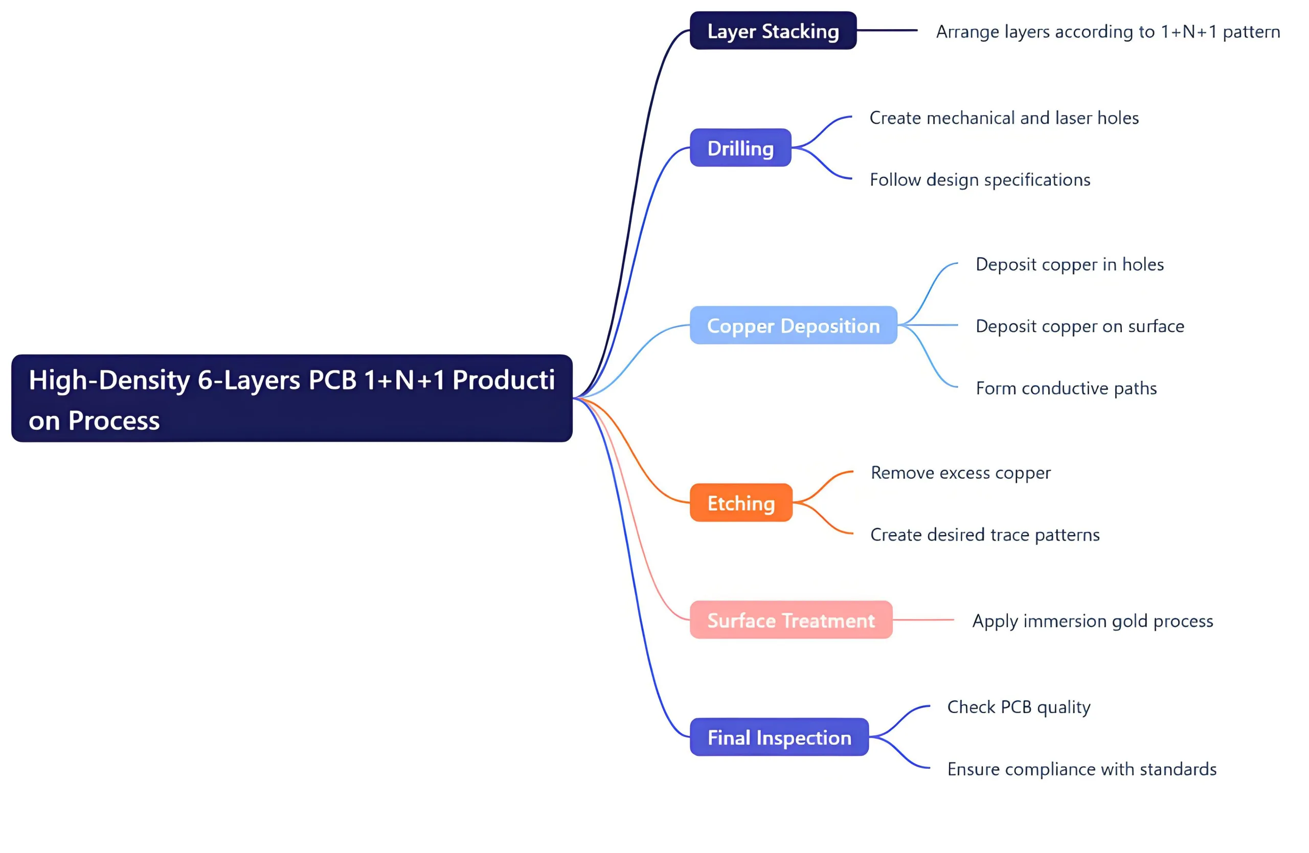
생산 과정
- 레이어 스태킹: 1+N+1 패턴에 따라 6개의 레이어를 정확하게 배열합니다..
- 교련: 설계 사양에 따라 기계 및 레이저 구멍을 생성합니다..
- 구리 증착: 홀과 표면에 구리를 증착하여 전도성 경로를 형성합니다..
- 에칭: 과도한 구리를 제거하여 원하는 트레이스 패턴을 만듭니다.
- 표면 처리: 침지 골드 프로세스 적용.
- 최종검사: PCB의 품질을 확인하고 모든 표준을 충족하는지 확인하십시오..

사용 시나리오
모바일 메인보드 외에도, it can also be used in other small – form – factor electronic devices such as small portable media players or some compact Bluetooth devices where space is limited but reliable circuit connections are needed.