
제품개요
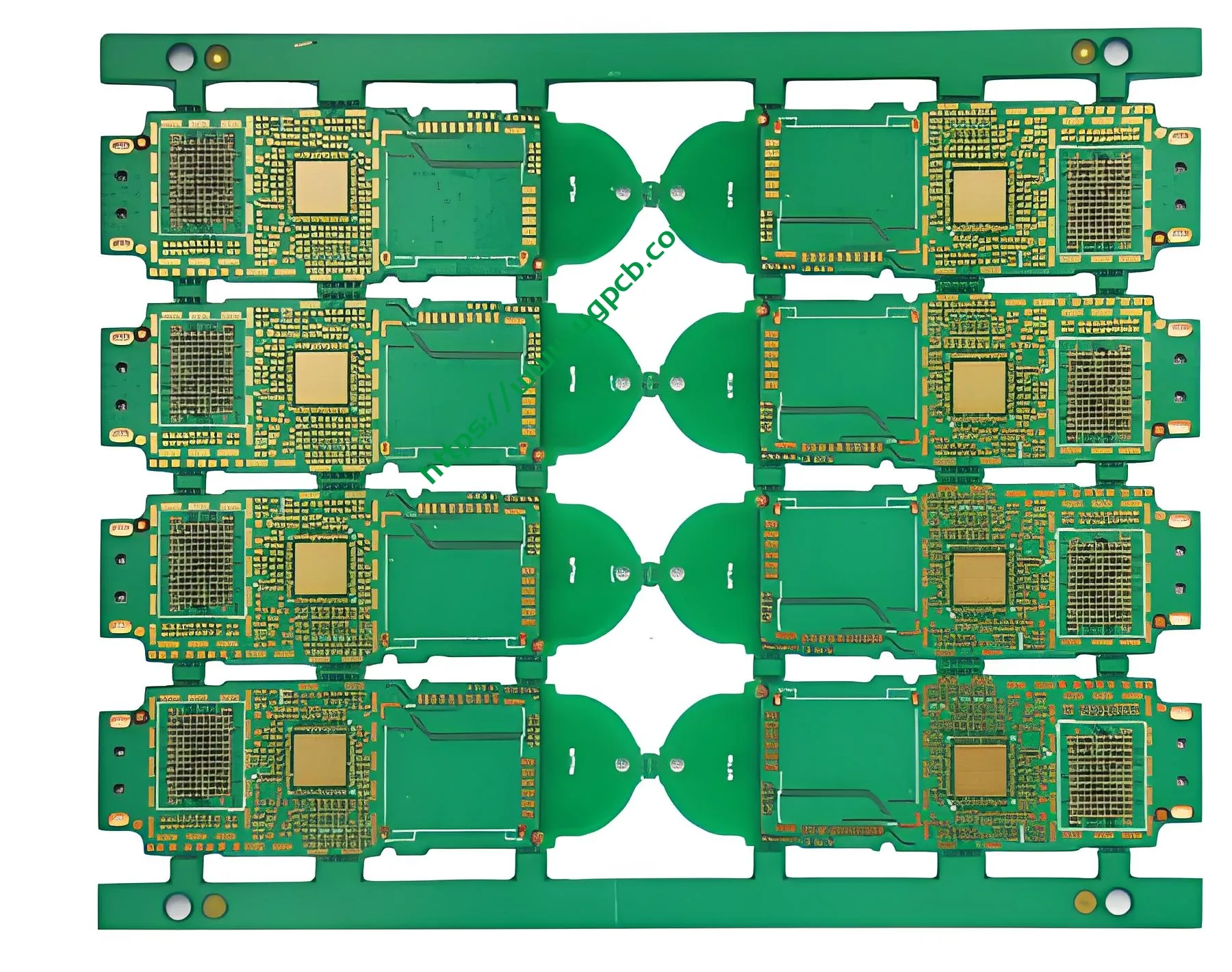
The 6L 1+N+1 HDI mobile mainboard is a high-density interconnect (HDI) 인쇄 회로 기판 (PCB) designed for use in mobile devices. With its advanced design and construction, this mainboard offers superior performance and reliability for demanding mobile applications.

정의
HDI stands for High-Density Interconnect, which refers to PCBs that have higher wiring density than traditional PCBs. The “1+N+1” designation indicates the layer structure of the PCB, with one power layer, N개의 신호 레이어, and one ground layer.
설계 요구 사항
The design of the 6L 1+N+1 HDI mobile mainboard must meet several key requirements:
- High signal integrity to support fast data transfer rates
- Low crosstalk and interference to ensure reliable communication
- Robust mechanical properties to withstand the stresses of daily use
- Thermal management to dissipate heat effectively
작동 원리
The 6L 1+N+1 HDI mobile mainboard operates by connecting various electronic components through a network of conductive pathways. These pathways are created using copper traces on the PCB layers, which are insulated from each other by layers of dielectric material. Electrical signals travel along these traces to perform the device’s functions.
목적 및 용도
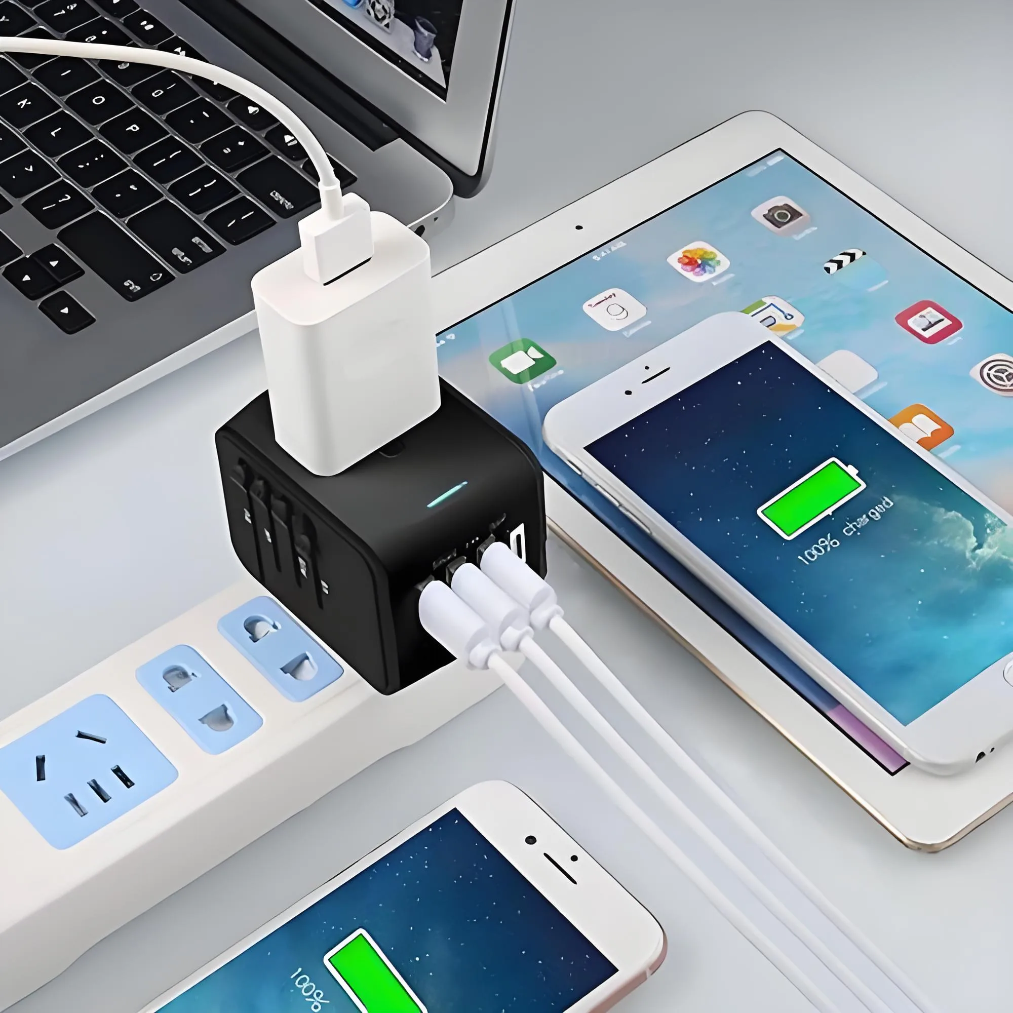
This type of mobile mainboard is commonly used in smartphones, 정제, and other portable electronic devices where space is limited but performance requirements are high. Its compact size and high functionality make it ideal for modern mobile technology.

분류
The 6L 1+N+1 HDI mobile mainboard falls under the category of high-end mobile mainboards due to its advanced features and construction. It is designed specifically for mobile applications requiring high performance and reliability.
사용된 재료
The main material used for this mainboard is FR-4, a flame-resistant glass-epoxy laminate composite. This material provides excellent thermal stability and mechanical strength, making it suitable for high-performance mobile applications.
성능 특성
- 높은 신호 무결성: Ensures fast data transfer rates without loss or distortion.
- Low Crosstalk: Minimizes interference between adjacent signal traces.
- 강력한 기계적 특성: Withstands the physical stresses of daily use.
- 효과적인 열 관리: Dissipates heat efficiently to prevent overheating.
구조와 특징
- 레이어 구조: Consists of six layers with a configuration of 1+N+1, where N represents the number of signal layers.
- 구리 두께: Inner layers have a thickness of 1 온스 (온스), while outer layers are 0.5 온스.
- 표면 처리: 이머젼 골드, 우수한 납땜성과 내식성을 제공하는 제품입니다..
- 최소 추적/공간: Capable of producing fine details with minimum trace widths and spaces of 3 밀.
- Hole Types: Mechanically drilled holes as small as 0.2 mm and laser-drilled holes as fine as 0.1 mm.
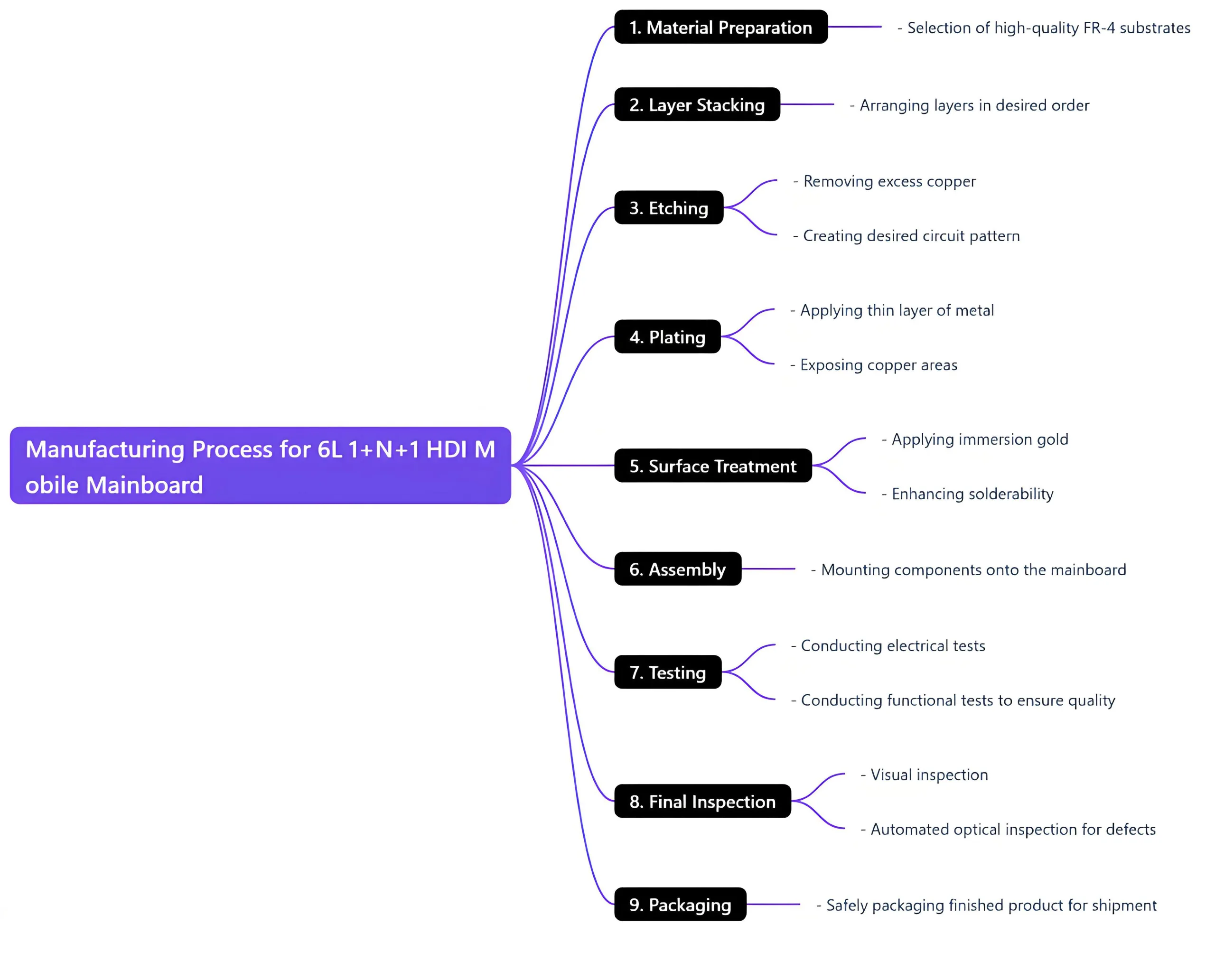
생산 과정
The manufacturing process for the 6L 1+N+1 HDI mobile mainboard involves several stages:
- 재료 준비: Selection of high-quality FR-4 substrates.
- 레이어 스태킹: Arranging the layers in the desired order.
- 에칭: Removing excess copper to create the desired circuit pattern.
- 도금: Applying a thin layer of metal to the exposed copper areas.
- 표면 처리: Applying immersion gold for enhanced solderability.
- 집회: Mounting components onto the mainboard.
- 테스트: Conducting thorough electrical and functional tests to ensure quality.
- 최종검사: Visual and automated optical inspection to check for defects.
- 포장: Safely packaging the finished product for shipment.

사용 사례 시나리오
- 가전제품: 스마트폰, 정제, 스마트워치, 등.
- 웨어러블 기기: Fitness trackers, health monitors, 등.
- 자동차 전자: In-car entertainment systems, navigation units, 등.
- 산업용 애플리케이션: 제어판, sensor interfaces, 등.
요약하면, the 6L 1+N+1 HDI mobile mainboard is an advanced PCB designed specifically for high-performance mobile applications. Its robust construction, 뛰어난 신호 무결성, and efficient thermal management make it an ideal choice for modern mobile technology.