


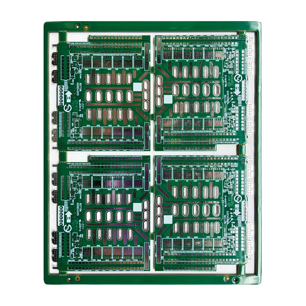
High-Reliability 8-Layer Rigid PCB 제품개요 & 정의
In the realm of high-speed, high-density electronic design, 다층 PCB (인쇄 회로 기판) are indispensable. UGPCB 8-레이어 견고한 PCB, built with a substantial 2.0mm 보드 두께 그리고 3OZ heavy copper foil, is engineered to withstand demanding electrical and physical environments. It serves not only as the foundation for electrical connectivity but as a critical component ensuring device stability and enhanced product reliability. For applications in industrial controls, power systems, 아니면 자동차 전자제품, this high-specification board is the optimal solution for complex, high-performance designs.

핵심 사양
-
레이어 수: 8-레이어 리지드 PCB
-
완성된 보드 두께: 2.0mm ±10%
-
기본 재료: FR-4, 유리전이온도 (Tg) ≥ 170°C
-
표면 마감: 무연 열풍 솔더 레벨링 (HASL-LF)
-
구리 무게: 3 평방 피트 당 온스 (≈105μm) for both inner and outer layers
-
솔더 마스크 & 실크 스크린: Green LPI Solder Mask, White Silkscreen Legend
중요한 설계 고려 사항
When designing with this high-specification PCB, engineers must prioritize:
-
열 관리: Leverage the high current-carrying capacity of 3OZ heavy copper to optimize power and ground planes, reducing impedance and heat rise. Use thermal simulation in conjunction with the high heat resistance of FR-4 TG170 material.
-
임피던스 제어 & 신호 무결성: The 8-layer stack-up allows effective separation of signal, 힘, 그리고지면 층. Precise calculation and control of trace impedance (예를 들어, 50Ω 단일 종단, 100Ω 차동) is essential to minimize reflection and crosstalk.
-
기계적 & Electrical Reliability: 그만큼 2.0mm thick board enhances overall rigidity, suitable for applications with vibration or insertion stress. For high-voltage or high-current nodes, adjust trace width and clearance according to IPC-2221 standards 그리고 3OZ copper weight to ensure safety margins.
-
DFM (제조 가능성을위한 설계): Collaborate with UGPCB’s engineering team early to address specific requirements for heavy copper PCB 그리고 thick board PCB 처리, such as drilling parameters and plating uniformity, ensuring a high-yield manufacturing process.
작동 방식 & 구조
안 8-레이어 PCB is fabricated by laminating multiple conductive layers into a single unit using precise processes including inner-layer imaging, 라미네이션, 교련, 그리고 도금. Electrical connections between layers are established via 도금된 관통 구멍 (PTHS), 블라인드 비아, or buried vias. A typical stack-up example is:
최상층 (신호) — Prepreg — L2 (지면) — Core — L3 (신호) — Core — L4 (힘) — Core — L5 (신호) — Prepreg — Bottom Layer (신호)
This “sandwich” structure effectively isolates high-speed signals, provides solid reference planes, and ensures efficient power distribution.
성능 & 주요 특징
-
Superior Electrical Performance: 3OZ heavy copper provides extremely low conductor resistance and excellent current-carrying capacity (over 3x that of standard 1OZ copper), reducing power loss and voltage drop.
-
Exceptional Thermal Reliability: FR-4 TG170 high Tg material withstands higher operating and soldering temperatures. Combined with the thermal conductivity of heavy copper, it significantly improves long-term reliability in high-temperature environments.
-
Enhanced Mechanical Stability: 그만큼 2.0mm thick board combined with rigid FR-4 offers superior resistance to bending and vibration, ideal for harsh operating conditions.
-
High Solder Joint Reliability: 그만큼 HASL-LF surface finish 아파트를 제공합니다, coplanar pad surface with excellent solderability and extended shelf life, compliant with RoHS directives.
-
고밀도 상호 연결 (HDI) 능력: The 8-layer design offers ample routing space for complex circuits, facilitating device miniaturization and functional integration.
생산 공정 개요
Engineering Review → Material Cutting (FR-4 TG170) → Inner Layer Imaging & 에칭 (3온스) → Oxide Treatment & Lamination → Mechanical Drilling & Copper Plating → Outer Layer Patterning & 도금 (to 3OZ) → 솔더 마스크 적용 (Green LPI) & 실크 스크린 (하얀색) → Lead-Free HASL Surface Finish → Electrical Testing & 최종검사 (per IPC standards)
Each stage incorporates stringent quality control checkpoints to ensure every high-reliability multilayer PCB meets exact customer specifications.
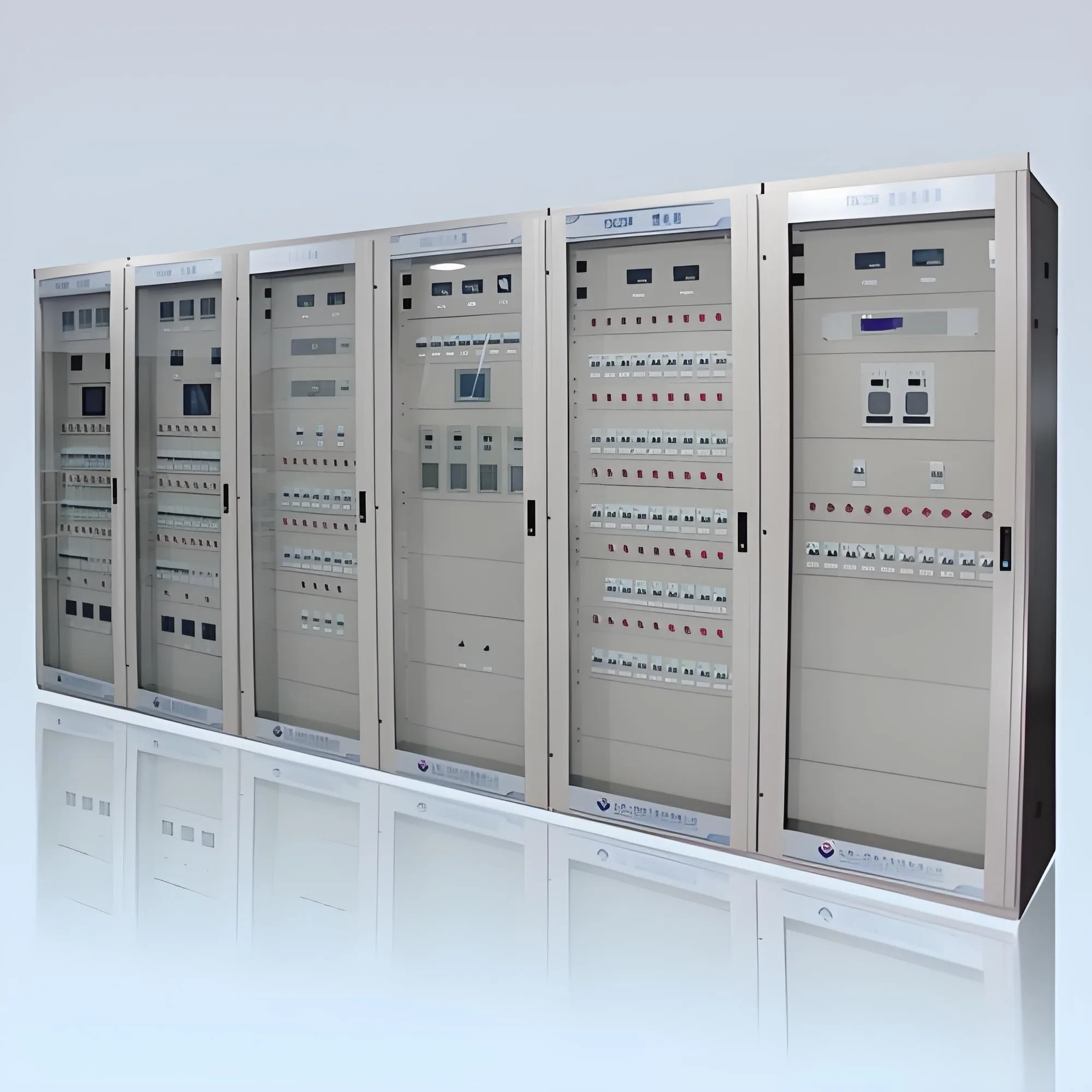
기본 응용 프로그램 & 사용 사례
This PCB is designed for high-power, high-stability applications:
-
산업 제어 시스템: plcs, 모터 드라이브, and industrial power supplies requiring heavy copper PCBs for high current.
-
재생 에너지 & Power Systems: Solar inverters, UPS 시스템, and EV charging modules relying on high current capacity and thermal endurance.
-
자동차 전자: On-Board Chargers (OBC), 배터리 관리 시스템 (BMS), and DC-DC converters, 어디 high Tg PCBs are essential for under-hood temperatures.
-
통신 인프라: Base station power amplifier units and network backup power systems.
-
고급 테스트 & 측정 장비: Instruments requiring stable power delivery and low-noise performance.

제품 분류 (Per IPC Standards)
-
레이어 수에 의해: 다층 PCB (>4 레이어), specifically an 8-layer circuit board.
-
강성별: 강성 PCB.
-
기본 재료에 의해: FR-4 PCB, subset: 높은 TG PCB (Tg ≥ 170°C).
-
By Special Process: 무거운 구리 PCB (per IPC-2152), Thick Board PCB.
-
애플리케이션 클래스별: Suitable for IPC 클래스 2 (Dedicated Service Electronic Products) 그리고 수업 3 (High-Reliability Electronic Products) 애플리케이션, 포함 Industrial Grade PCB, Power Electronics PCB, 그리고 Automotive Grade PCB.