

In today’s rapidly evolving 5G communications, 레이더, and satellite navigation sectors, the performance of RF PCB directly dictates the signal quality and stability of end devices. Facing the classic engineering dilemma of “ultimate high-frequency performance” versus “strict cost control,” UGPCB introduces the 로저스 RO4003C + FR4 혼합 유전체 RF PCB. This innovative product not only retains the excellent high-frequency characteristics of Rogers materials but also, through a clever hybrid laminate structure, provides you with a highly cost-effective system-level solution.


1. 제품개요: Defining the Next Generation of Communication Equipment PCBs
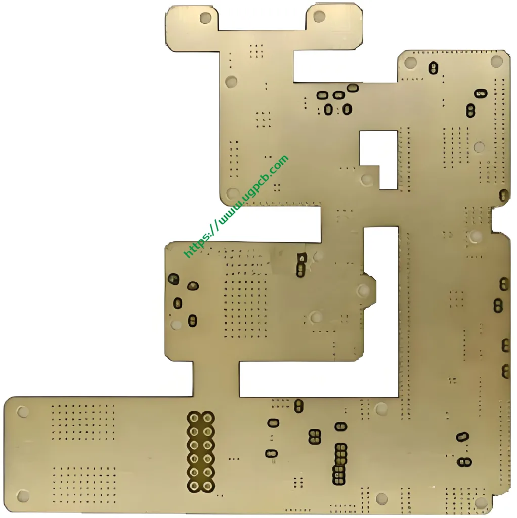
그만큼 로저스 RO4003C + FR4 혼합 유전체 RF PCB from UGPCB is a 4-layer 인쇄 회로 기판 engineered specifically to integrate high-frequency RF circuits with low-speed digital control circuitry on a single substrate. It innovatively combines two layers of Rogers RO4003C high-frequency laminate with two layers of standard FR-4 material through an advanced lamination process.
-
모델: 로저스 RO4003C + FR4 혼합 유전체 RF PCB
-
레이어 수: 4 레이어
-
유전 상수 (DK): 3.38
-
Target Applications: 통신 장비, 기지국 안테나, RF front-end modules
2. 제품 정의 & 디자인 고려 사항: What is a Mixed Dielectric PCB?
에이 mixed dielectric PCB, also known as a 하이브리드 PCB, refers to a circuit board that incorporates two or more different types of laminate materials within its construction. For this specific product, the core design consideration lies in the seamless integration of the high-performance but higher-cost Rogers RO4003C with the ubiquitous and economical FR-4.
The defined stack-up structure is “2 Layers Rogers RO4003C + 2 Layers FR-4.” The top layer and critical signal layers utilize Rogers material to handle RF signals, while the bottom layer and power planes use FR-4 for low-frequency logic and power distribution. During the design phase, precise impedance matching is paramount. Engineers must leverage the stable 유전 상수 (DK: 3.38) ~의 로저스 RO4003C to meticulously control the characteristic impedance of RF traces (예를 들어, 50Ω ±10% or 100Ω differential), thereby ensuring signal integrity.
3. 작동 원리, 재료 특성, & 성능: Why Choose RO4003C?
3.1 Core Material Analysis
-
로저스 RO4003C: This is not a traditional PTFE (폴리테트라플루오로에틸렌) 재료. It is a ceramic-filled hydrocarbon thermoset laminate reinforced with woven glass. Its key attributes include a stable 유전 상수 (DK) ~의 3.38 with excellent lot-to-lot consistency across a wide frequency range and a very low 소산 인자 (Df) ~의 0.0027 ~에 10 GHz, which minimizes signal energy loss . 결정적으로, it is designed to be processed using standard epoxy/glass (FR-4) fabrication techniques, eliminating the need for specialized via preparation like sodium etching required for PTFE materials, thus supporting lower manufacturing costs .
-
FR-4: As the industry-standard epoxy glass-reinforced laminate, FR-4 provides excellent mechanical support, thermal dissipation pathways, and compatibility with mature PTH (Plated Through-Hole) 프로세스, all at a significantly lower cost compared to high-frequency materials.
3.2 핵심 성능 매개 변수
-
완성된 보드 두께: Precisely controlled at 1.0 mm, meeting the slim profile requirements of modern communication modules .
-
유전체 두께: 0.508 mm provides a precise physical foundation for RF trace impedance calculations .
-
Finished Copper Thickness Distribution: 1/0.5/0.5/1 (온스). The outer layers utilize 1 oz copper to meet soldering and current-carrying requirements, while the inner layers use 0.5 oz copper to facilitate finer line resolution .
-
Copper Foil Type: ½ oz (18μm) HH/HH 구리박. This denotes reverse-treated foil (RTF) 양쪽에. RTF features a profiled (거친) side for enhanced adhesion to the dielectric and a smooth side for reduced conductor loss, thereby improving insertion loss and overall signal integrity .
-
표면 마감: 이머젼 골드 (동의하다) . This finish provides excellent surface planarity, superior solderability, and long-term corrosion resistance, making it ideal for high-precision RF solder joints and potential wire bonding applications .
4. 제조공정: Technical Challenges of Hybrid Lamination
Fabricating a 로저스 RO4003C + FR4 hybrid PCB is far more complex than simply stacking two different materials. The engineering team at UGPCB meticulously controls the following core processes to ensure final product yield and long-term reliability:
-
Material Pre-treatment: The RO4003C cores undergo baking (예를 들어, at 120°C) to remove moisture. Plasma treatment is often applied to the material surfaces to enhance surface energy and promote robust bonding with the prepreg materials.
-
Inner Layer Imaging: 활용 LDI (레이저 직접 이미징) 기술, inner layer circuits are accurately defined, with critical RF trace width tolerances controlled to within +/-0.025mm.
-
The Critical Lamination Process:
-
재료 쌓기: The layup is strictly controlled to follow the “2L RO4003C + 2L FR4” sequence.
-
Bonding Material Selection: Appropriate prepregs, such as Rogers 4450F bond ply or low-flow FR-4 prepregs, are selected to prevent excessive resin flow that could lead to uneven dielectric thickness .
-
Lamination Parameters: A stepped or multi-stage temperature cure cycle is employed. The process must balance the higher lamination temperature requirements of RO4003C (대략. 190-200℃) with those of FR-4 (대략. 170-185℃). A carefully controlled ramp-up rate (예를 들어, 1.5°C/min) is critical to mitigate the risk of delamination caused by the differing coefficients of thermal expansion (CTE) between the two material types.
-
-
Mechanical Drilling & 도금: Given the ceramic-filled nature of RO4003C, carbide drills with optimized speed and feed rates are used to ensure smooth, smear-free hole walls. The subsequent electroless copper plating and electrolytic plating processes ensure uniform copper deposition within the vias, guaranteeing reliable interlayer connections.
-
외층 & 솔더 마스크: After outer layer imaging and etching, the Immersion Gold (동의하다) surface finish is applied. Nickel and gold thicknesses are strictly controlled to prevent “gold embrittlement” and ensure reliable RF contact performance .
5. 제품 분류 & 응용 시나리오
기술적으로, this product falls under the category of “Rigid Multilayer Mixed Dielectric High-Frequency PCBs” .
Its unique material structure makes it exceptionally suitable for the following 애플리케이션 시나리오:
-
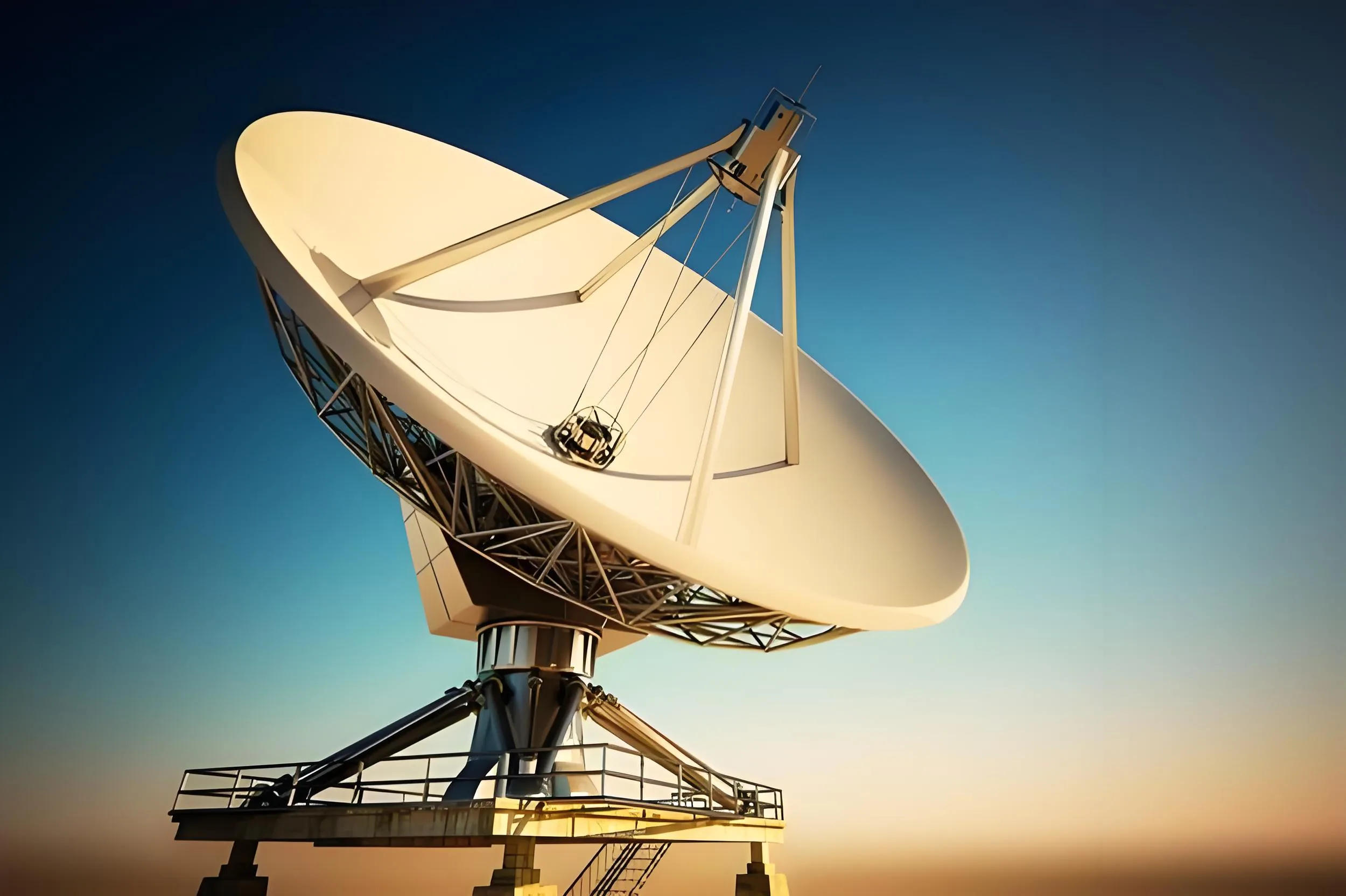
Wireless Communication Infrastructure: Such as 5G Small Cells and Remote Radio Units (RRUs). Antenna arrays and filter circuits benefit from the low-loss properties of RO4003C, while the control and power management sections utilize the cost-effective FR-4.
-
자동차 전자: 77 GHz radar sensors and ADAS (고급 운전자 지원 시스템) modules require stable dielectric constant performance at high frequencies for accurate distance and velocity detection .
-
RFID & 위성 통신: GPS receivers, satellite TV LNB (Low-Noise Block Downconverters) demand extremely low signal latency and noise figures, which the RO4003C layer helps achieve.
-
High-End Consumer Networking: High-performance routers and access points leverage this technology to meet the increasing signal integrity demands of Wi-Fi 6/6E/7, ensuring robust coverage and data throughput.

6. Why Choose UGPCB’s Hybrid Dielectric Solution?
-
The Ultimate Performance vs. 비용 균형: Compared to a full-build using Rogers material across all layers, 그만큼 RO4003C + FR4 hybrid structure significantly reduces material costs by restricting the expensive high-frequency laminate to only the critical signal layers. This embodies the design philosophy of “maximizing value where it matters most.”
-
Precision Impedance Control: Leveraging our deep understanding of the material’s Dk (3.38) and precise control over dielectric thickness (0.508mm), UGPCB delivers controlled impedance with tolerances consistently held to ±10% or tighter.
-
엔드 투 엔드 기술 지원: From material selection guidance and stack-up calculation to final PCB 제작, the experienced engineering team at UGPCB provides comprehensive support, helping you navigate potential design pitfalls and ensuring your product’s success.
7. 행동을 취하십시오: Get Your Custom Quote Today
Whether you are engineering the next generation of 5G base station antennas or designing high-precision automotive radar systems, UGPCB 로저스 RO4003C + FR4 혼합 유전체 RF PCB is the most reliable hardware foundation for your innovation.
Don’t let your 회로 기판 be the bottleneck in your product’s performance!
이메일: sales@ugpcb.com
Our experienced engineers will review your design files within 24 hours and provide a comprehensive DFM (제조 설계) analysis along with a highly competitive quotation.