

고속, 고주파 전자공학의 세계, 도금의 모든 미크론과 표면 평탄도의 모든 측면이 신호 전송 순도와 최종 제품 신뢰성을 직접적으로 결정합니다.. AI 서버 등 최첨단 분야로, 새로운 에너지 자동차 전자, 5G 통신은 점점 더 엄격한 성능 요구를 요구합니다. 인쇄 회로 기판 (PCB), 전통적인 표면 마감 공정은 한계에 직면해 있습니다.. 응답으로, UGPCB has made a significant investment and officially launched an industry-leading “Fully Automated ENIG (이머젼 골드) Post-Processing Line.” This is not merely an equipment upgrade but a solemn commitment to providing comprehensive reliability solutions for high-end PCB (인쇄 회로 보드 어셈블리) 고객, 기판부터 완제품까지.
동의 프로세스: 고급 PCB 제조를 위한 필수 선택인 이유?
다양한 PCB 표면 마무리 공정 중, 무전해 니켈 침지 금 (동의하다) 독특한 물리적, 화학적 특성으로 인해 눈에 띕니다.. ENIG 공정은 단순히 구리 표면을 금층으로 덮는 것이 아닙니다.. 먼저 구리 표면에 장벽으로 조밀한 니켈-인 합금층을 화학적으로 증착하는 복합 공정입니다., 그 후 니켈층 위에 고순도 금층을 치환 증착.
고주파용, 고속 PCB 제조 및 고밀도 상호 연결 (HDI) 무대, ENIG의 장점은 대체할 수 없습니다:
-
탁월한 신호 무결성: ENIG는 패드만 정확하게 커버합니다., 구리층을 주요 신호 전송 매체로 남겨두기. This effectively avoids “skin effect” losses in high-frequency signal transmission, 이는 밀리미터파 레이더 보드 및 GPU 상호 연결 보드에 매우 중요합니다..
-
우수한 표면 평탄도: 금층은 균일한 두께로 증착됩니다., BGA 및 QFN과 같은 미세 피치 구성요소의 SMT 조립을 위해 거의 완벽에 가까운 평평한 표면을 제공합니다., 솔더 보이드 및 툼스토닝과 같은 결함을 크게 줄입니다..
-
연장된 보관 수명 및 납땜성: ENIG 보드는 산화에 강합니다., 유통기한이 초과된 12 개월 - HASL보다 훨씬 길다 (3-6 달) 및 OSP 프로세스. 이는 부품 조달 및 생산 일정에 대한 뛰어난 유연성을 제공합니다..
-
우수한 접착 및 접촉 성능: 고순도 금 표면은 금 와이어 본딩에 이상적인 인터페이스를 제공하며 낮은 품질을 보장합니다., 골드 핑거와 같은 부품의 안정적인 접촉 저항.
테이블 1: 주요 PCB 표면처리 공정 비교
| 프로세스 유형 | 동의하다 (이머젼 골드) | HASL (무연) | OSP (유기 용해성 보존) |
|---|---|---|---|
| 평탄 | 훌륭한, 미세 피치 부품에 적합 | 가난한, prone to “tin whiskers” | 훌륭한 |
| 유통기한 | >12 달 | 3-6 달 | ~6개월 (엄격한 습도 관리가 필요합니다) |
| 납땜 가능성 | 훌륭한, 여러 리플로우 사이클에 대해 안정적 | 좋은 | 좋은, 그러나 제한된 리플로우 주기 |
| 이상적인 애플리케이션 | 고주파, HDI, BGA, 골드 핑거스 | 소비자 전자 장치, 넓은 패드 | 저비용, 수명이 짧은 소비자 제품 |
| 환경 | 좋은 (시안화물이 없는 공정을 사용할 수 있습니다.) | 무연 규정 준수에 대한 높은 요구 사항 | 훌륭한 |
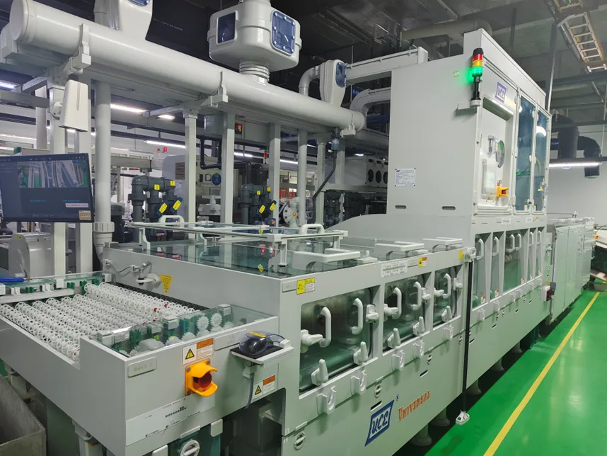
UGPCB의 ENIG 후처리 라인: 기술 매개변수 및 프로세스에 대한 심층 분석
UGPCB의 새로운 ENIG 후처리 라인은 지능형 제어와 정교한 관리 기능을 갖춘 수직 통합형 연속 생산 라인입니다.. 그 디자인은 표준 절차를 능가합니다., 모든 중요한 순간에 우리의 프로세스 전문성과 품질 약속을 통합합니다..
1. 전처리: 안정적인 접착의 기초
모든 우수한 도금층은 완벽한 구리 표면에서 시작됩니다.. 우리의 생산 라인은 다단계 정밀 세척 및 마이크로 에칭 시스템을 사용합니다.. 정밀하게 제어된 산성 과황산나트륨 용액 사용, 0.5-1.5μm의 최적 범위 내에서 구리 표면 마이크로 에칭을 유지합니다.. 이 단계는 매우 중요합니다. 구리 산화물을 철저하게 제거할 뿐만 아니라 균일한 표면을 생성합니다., 미세한 미세 거칠기, 후속 니켈층의 치밀한 접착을 위한 견고한 기반 마련.
2. 활성화 & 무전해니켈: 견고한 장벽층 구축
활성화는 ENIG 프로세스의 핵심입니다. 우리는 첨단 팔라듐 활성화 시스템을 활용합니다.. 팔라듐 이온 농도를 정밀하게 제어함으로써 (20-40 ppm) 그리고 온도 변동 (±1°C 이내), 우리는 구리 표면에 촉매 팔라듐 핵의 균일한 흡착을 보장합니다., eliminating the risk of “skip plating” or “leaching.”
후속 무전해 니켈 (안에) 도금은 솔더 조인트 신뢰성의 핵심 결정 요소입니다.. 최적화된 중인 산성 EN 공정을 사용합니다.. 증착된 니켈-인 합금층은 미세한 결정화가 특징입니다., 낮은 다공성, 안정적인 인 함량. 이 장벽은 구리와 금 사이의 확산을 효과적으로 방지합니다., inhibiting the formation of brittle “black nickel” (니켈-금 금속간화합물) 화합물. 이를 통해 장기간 사용하거나 고온 환경에 노출된 후에도 솔더 조인트가 견고하고 안정적으로 유지됩니다..
3. 이머젼 골드: 최종 보호 표면
금 침지 단계에서, UGPCB는 매우 안정적인 시안화물이 없는 침지 금 공정을 채택합니다., 친환경성과 성능의 최적의 균형 달성. 최종 표면층으로서, 금의 순도와 두께가 중요합니다. 우리의 공정은 금층 순도가 99.95%, 0.05-0.3μm 사이에서 정밀하게 제어되는 두께, 밝은 레몬옐로우 컬러를 표현하고 있어요. 이 얇은, 조밀한 금층은 우수한 내산화성과 접촉 성능을 제공하는 동시에 지나치게 두꺼운 금층으로 인한 솔더 조인트 취성을 방지합니다..
지능형 제어 & 품질 보증: 하드웨어를 넘어선 경쟁력
하드웨어는 뼈대이다, 하지만 지능형 공정 제어는 생산 라인의 중추입니다.. UGPCB ENIG 후가공라인의 핵심경쟁력이 여기에 담겨있습니다.:
-
MTO (금속 회전율) 지능형 포카요케 시스템: 특허기술과 유사한 선진화된 관리시스템을 구현하였습니다.. 핵심 생산 모델 기반 (예를 들어, W = TλNCθ와 같은 매개변수가 포함됩니다., 여기서 W는 총 금 중량입니다., T는 시간이다, 및 λ, 기음, θ는 제품/효율성 관련 매개변수입니다.) 각 배치의 ENIG 면적 및 수량과 결합됩니다., 시스템은 금 탱크의 실제 MTO 값을 자동으로 계산합니다.. 생산 전, 실제 값을 표준과 비교합니다.. 미리 설정된 MTO에 도달하거나 초과되면, the system “poka-yokes” (실수 방지) 일괄 로드를 잠그고 금지하여. 이는 솔더 패드가 젖지 않거나 화학 수명 소모로 인한 부식과 같은 위험을 근본적으로 방지합니다., 모든 보드가 최적의 화학 활동 창 내에서 처리되도록 보장.
-
전체 프로세스 디지털 매개변수 모니터링: 이 라인에는 실시간 데이터 수집과 폐쇄 루프 온도 제어를 수행하는 중앙 모니터링 시스템이 통합되어 있습니다., ph, 집중, 모든 탱크의 침수 시간 (청소, 마이크로 에칭, 활성화, 니켈, 금, 등.). 모든 데이터는 추적 가능합니다., providing a “data fingerprint” for process stability and quality consistency.
-
최적화된 후처리 헹굼: 고품질 ENIG 요구 사항을 엄격하게 준수, 주요 공정 이후 충분한 역류 다단계 헹굼을 구성했습니다.. 후속 탱크의 구리 이온 오염을 방지하기 위해 마이크로 에칭 후 린스의 청결성에 특별한 주의를 기울입니다., 이는 팔라듐 활성화욕의 수명에 영향을 미칠 수 있습니다..
미래를 위한 역량 강화: UGPCB ENIG 프로세스의 산업 응용 및 노력
이 고급 ENIG 후처리 라인 활용, UGPCB는 고객에게 실질적인 가치 향상을 제공합니다.:
-
고주파 애플리케이션 문제 극복: 자동차 밀리미터파 레이더 보드에 신호 손실을 최소화한 표면 마감 솔루션 제공, 5G 안테나 보드, 및 AI 서버 백플레인, Rogers와 같은 고급 라미네이트의 공정 요구 사항 충족.
-
초고밀도 설계 지원: 조립 요구 사항을 완벽하게 지원합니다. 01005 소형 부품 및 0.2mm 미세 피치 BGA, 웨어러블 장치 및 고급 의료 전자 PCBA에 이상적입니다..
-
장기적인 신뢰성 보장: 탁월한 내산화성 및 내식성은 까다로운 산업 분야에서 탁월한 성능을 보장합니다., 자동차 전자, 항공우주 환경.
-
빠른 응답 & 일관성: 완전 자동화된 라인은 매우 높은 공정 반복성과 안정성을 보장합니다., 원활한 전환 지원 PCB 프로토타입 제조 대량 PCBA 생산, 유리한 리드타임 제공.
결론
영역에서는 PCB 제조, 정밀도는 미크론 단위로 측정됩니다., the refinement of every process detail represents a responsibility toward our customers’ product reliability. UGPCB의 새로운 ENIG 후처리 라인 시운전은 고급 PCB 제조 및 PCBA 조립의 새로운 단계로의 진입을 의미합니다.. 우리는 단순한 회로 기판이 아닌 제품을 제공합니다, 하지만 성능 보장, 신뢰할 수 있음, 그리고 신뢰. 우리는 업계 파트너와 고객을 방문하여 당사의 프리미엄 PCB 제조 및 PCBA 조립 서비스가 어떻게 차세대 주력 제품의 성공을 보호할 수 있는지 논의할 수 있도록 정중히 초대합니다..