
In compact power modules, new energy vehicle control units, or high-power industrial equipment, PCB designers often face a severe challenge: how to safely manage high voltage within limited board space? A seemingly minor spacing design error can lead to arc discharge, insulation failure, or even safety incidents. This article provides an in-depth analysis of two core concepts in high voltage routing — Clearance and Creepage Distance — and establishes a robust safety foundation for your PCB and PCBA design based on authoritative standards.
Concept Clarification: The Fundamental Difference Between Clearance and Creepage
First, we must clearly define these two frequently confused safety concepts. According to IPC-2221B (Generic Standard on Printed Board Design) and IEC 60664-1 (Insulation Coordination for Equipment Within Low-Voltage Systems):
-
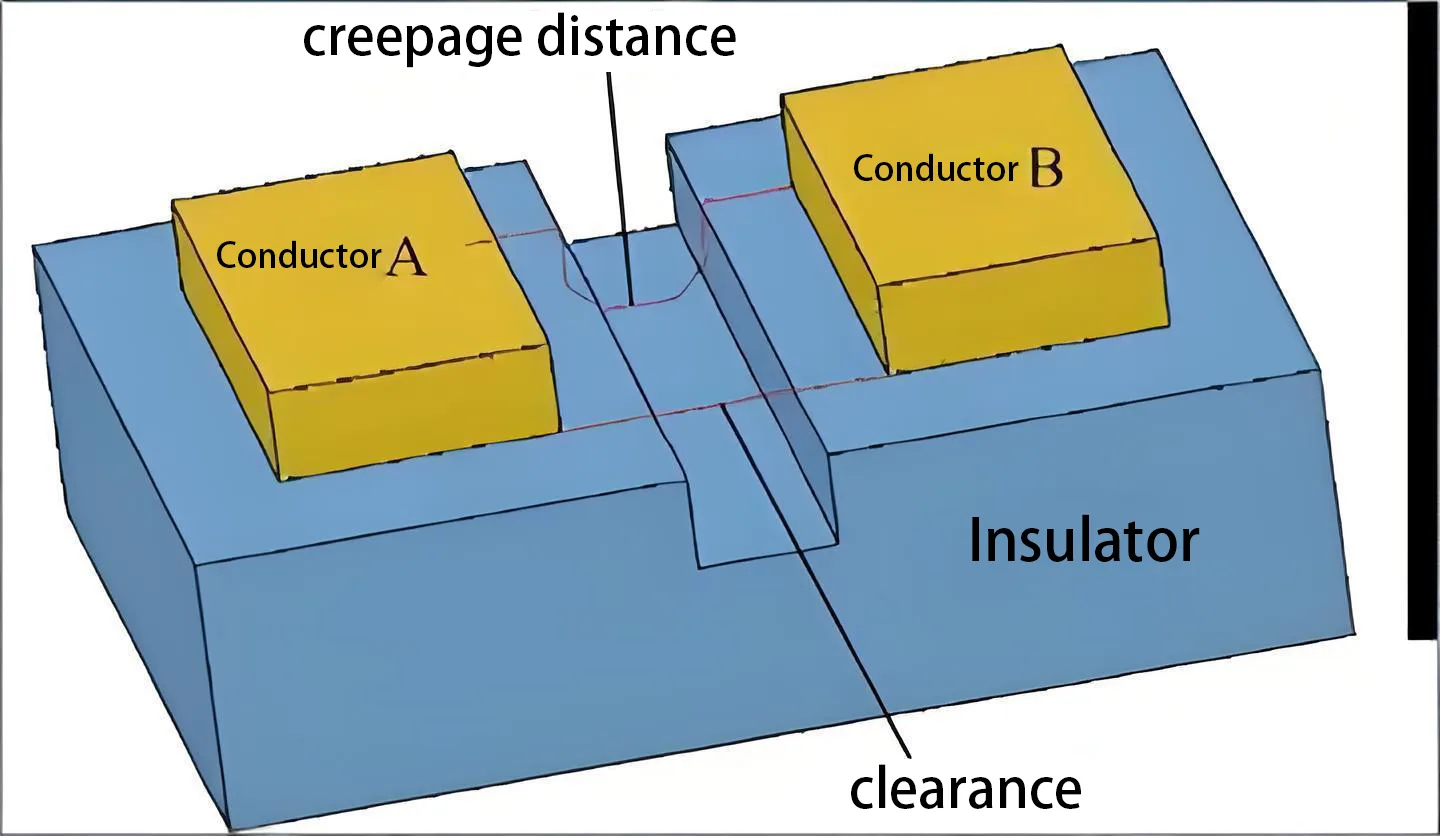
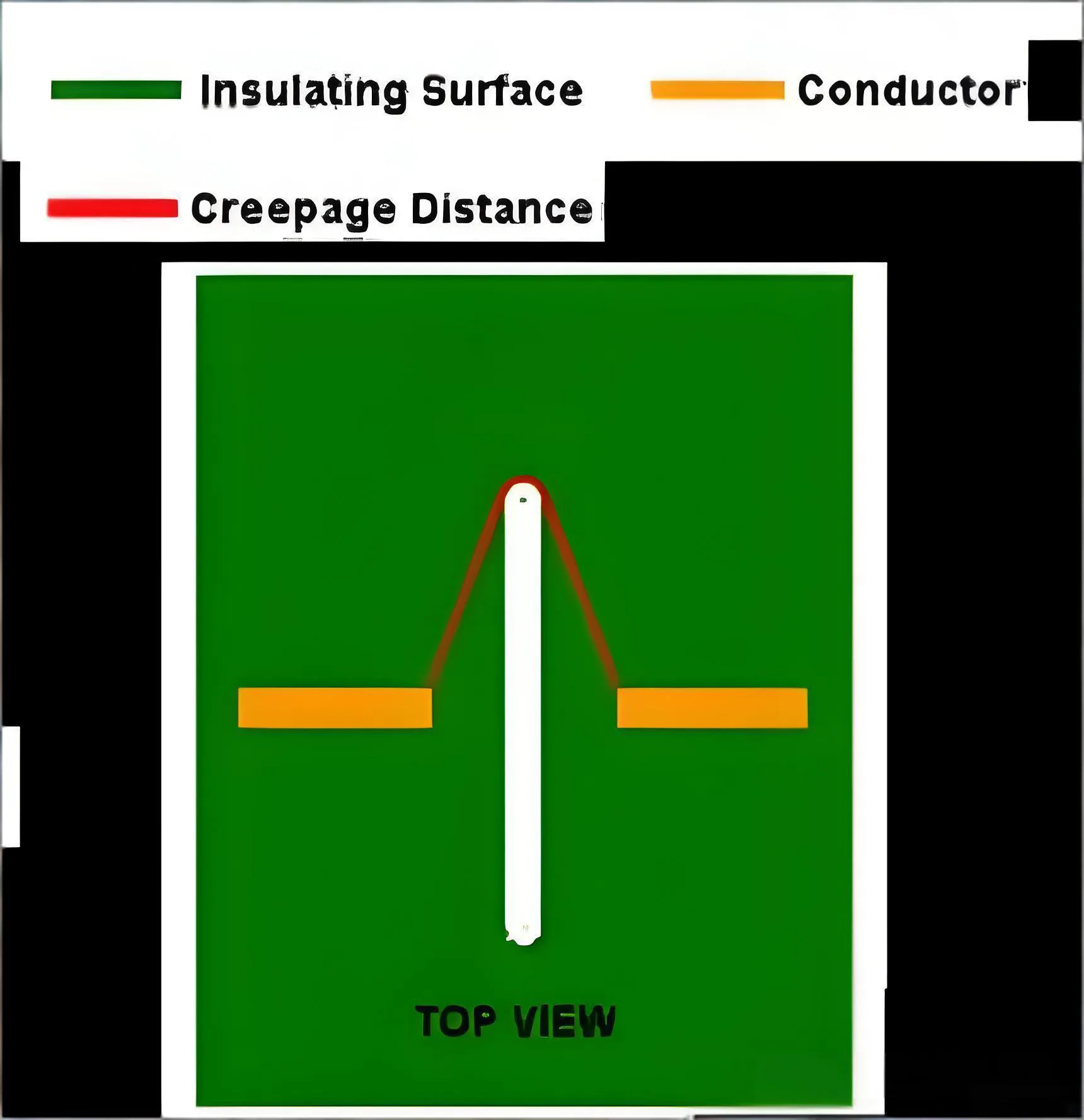
Clearance: The shortest straight-line distance in air between two conductive parts, or between a conductive part and the equipment enclosure. It primarily prevents the air dielectric from being broken down by high voltage, causing instantaneous arcing. Think of it as the “straight-line distance to fly across a canyon.”
-
Creepage Distance: The shortest path length along the surface of an insulating material between two conductive parts. It primarily prevents contaminants (such as dust, moisture, flux residue) from forming a conductive path on the insulation surface, leading to slow leakage or tracking failure. This is akin to the “shortest path for an ant to crawl along the canyon wall.”
The core distinction lies in the medium: one relies on air, the other concerns the condition of the insulation surface. In environments with higher pollution degrees, creepage distance requirements are often more stringent than clearance.

Design Cornerstone: Authoritative Standards and Data-Driven PCB Design Specifications
Design without standards is blind. For high-voltage PCB design, engineers must follow corresponding safety standards (e.g., UL, IEC, GB) based on the product application field (such as consumer electronics, industrial control, medical devices, automotive electronics). Among these, IEC 60664-1 is a foundational international standard that provides a lookup table design method based on working voltage, pollution degree, material group, and overvoltage category.
Taking a typical AC-DC switching power supply (input 100-240VAC, with PFC circuit) safety isolation between primary and secondary sides as an example, its insulation requirements typically include:
-
Basic Insulation: Fundamental protection against electric shock.
-
Reinforced Insulation: Equivalent to double basic insulation, providing higher reliability.
According to IEC 62368-1 (Safety Standard for Audio/Video, Information and Communication Technology Equipment) and common certification requirements, under Pollution Degree 2 (general industrial environment), for a working voltage of 240VAC (corresponding peak voltage ~340V), the minimum creepage and clearance requirements are typically as follows:
| Insulation Type | Clearance (Min.) | Creepage Distance (Min., Material Group IIIa) |
|---|---|---|
| Basic Insulation | 2.0 mm | 3.2 mm |
| Reinforced Insulation | 4.0 mm | 6.4 mm |
(Note: The above are typical values. Actual design must follow the complete lookup table process of the chosen standard, considering factors like altitude and transient overvoltage.)

Solutions for Limited PCB Real Estate: Five Engineering Strategies
When board space is tight and straight-line distance requirements cannot be met, experienced PCBA design engineers employ the following strategies to effectively increase the creepage path length:
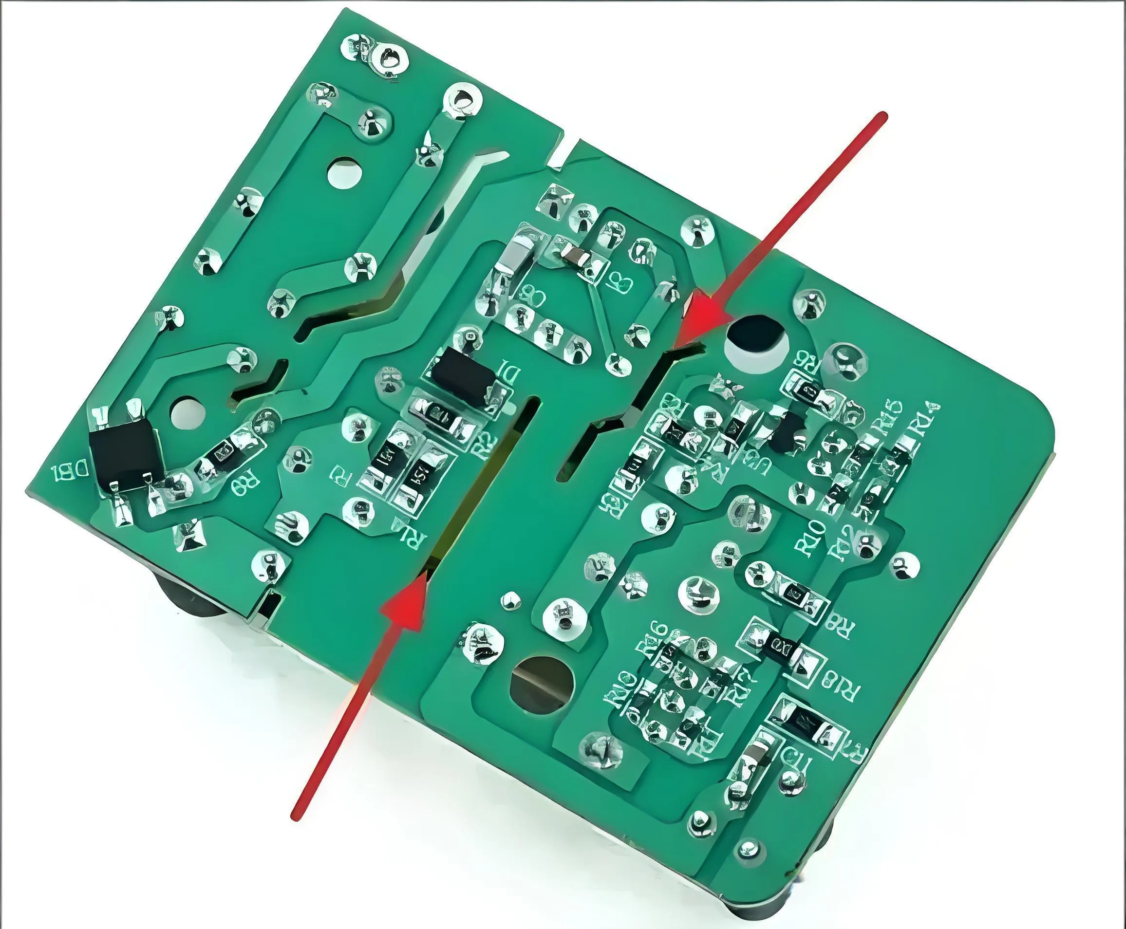
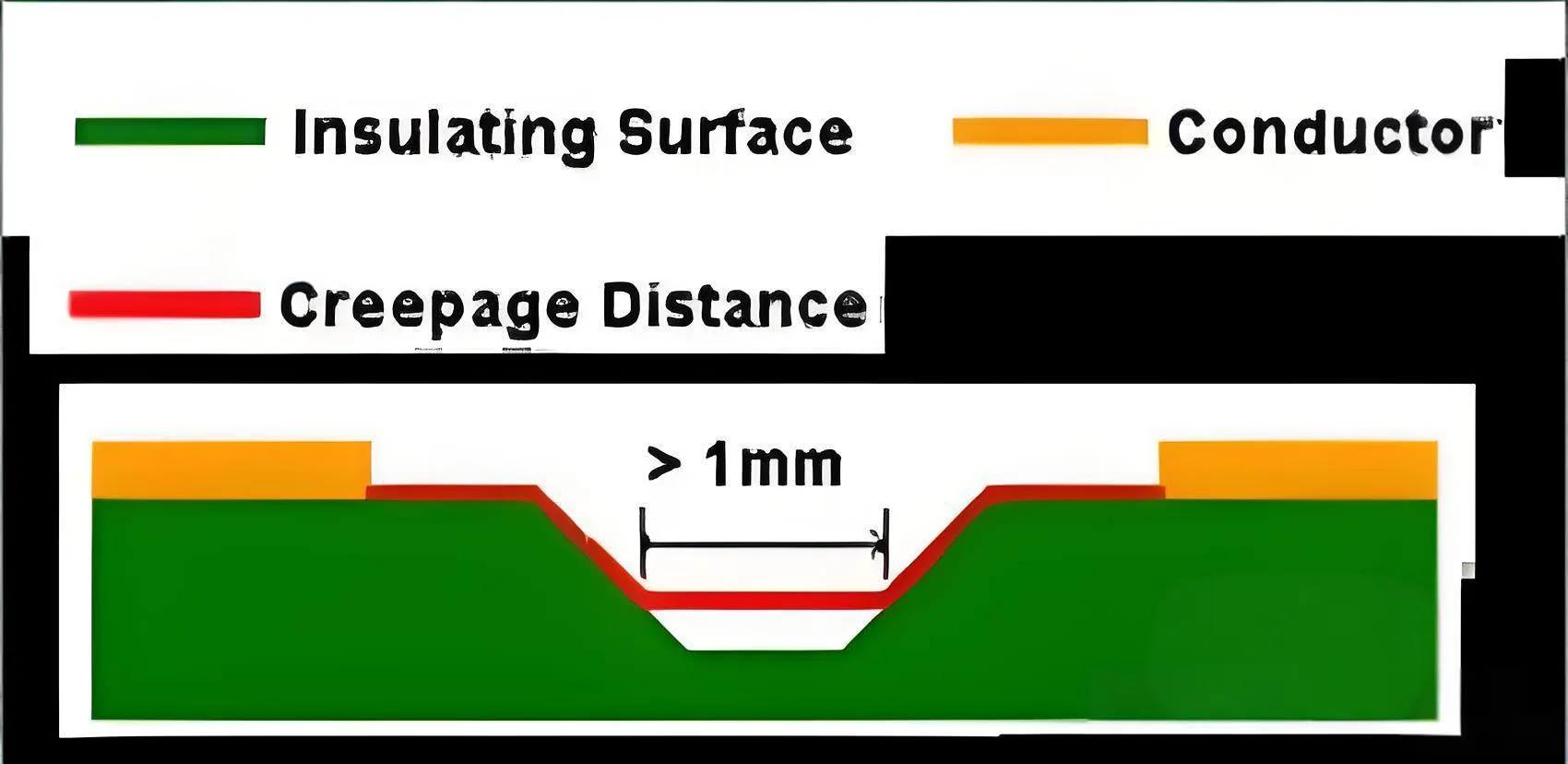
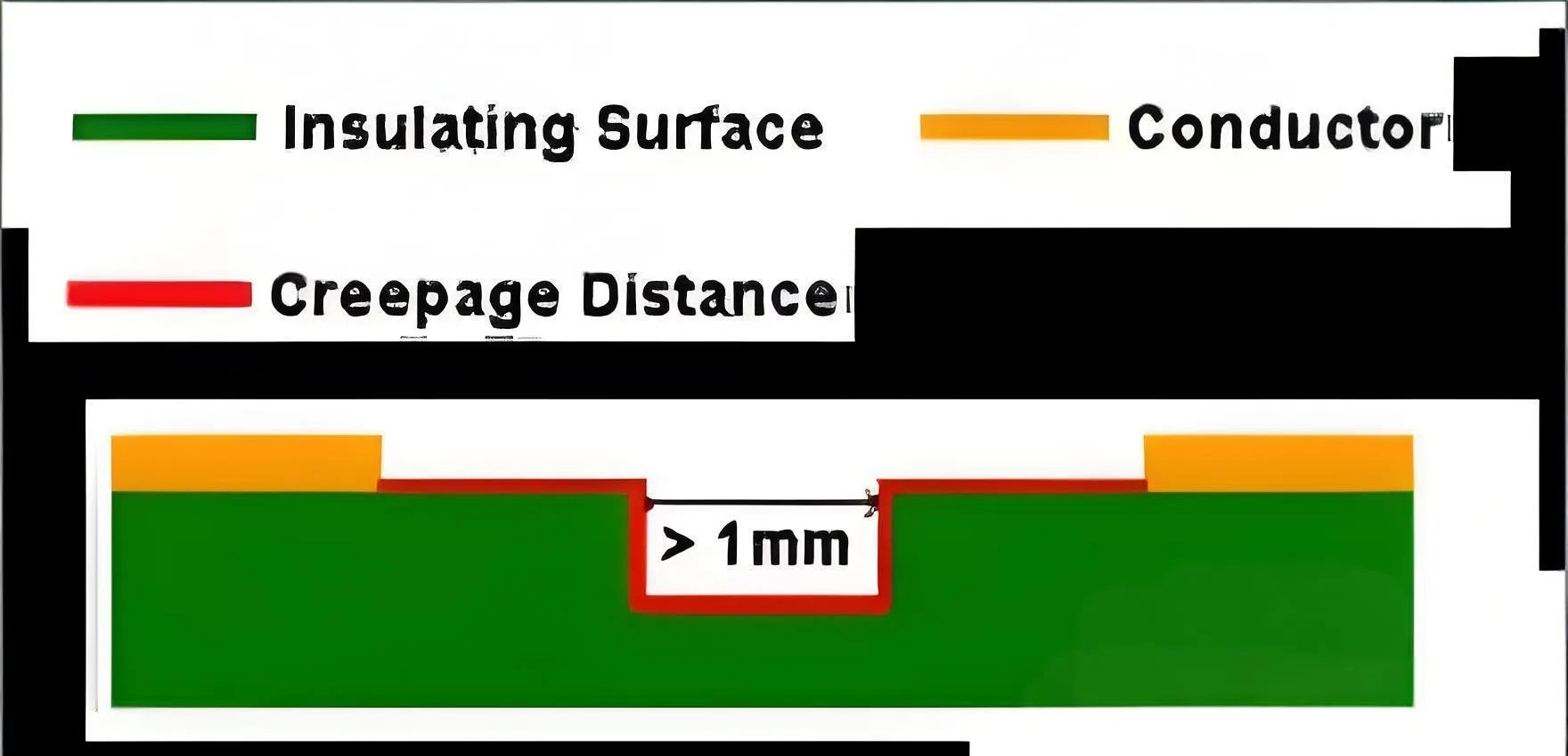
1. Slotting for Distance Increase
This is the most classic and effective engineering method. Mill or punch an isolation slot in the copper pour area between two high-voltage conductors.
-
V-Groove / U-Groove: Suitable for moderate distance compensation. The slot does not penetrate the PCB; depth is typically 1/3 to 2/3 of the board thickness. This effectively forces the creepage path to detour along the slot wall, significantly increasing surface distance.
-
Long Through-Slot: Most effective. A completely penetrating isolation slot (often width ≥1.0mm) is created directly between conductors. The creepage path must go around the entire slot length, increasing distance by more than twice the slot width. This is a common technique in switch-mode power supply PCBs for isolating primary from secondary sides.


2. PCB Material Upgrade
-
Select High-Performance PCB Substrate: The Comparative Tracking Index (CTI) of standard FR-4 typically ranges from 175-250V. Choosing high CTI materials (e.g., dedicated safety insulation materials with CTI ≥600V) allows for shorter creepage distance requirements per IEC standards. For instance, Material Group I (CTI ≥600V) can require nearly half the creepage distance of Group IIIa (100V ≤ CTI <175V).
-
Utilize Ceramic Substrates: For ultra-high power density designs, such as IGBT driver modules in automotive PCBs, directly use alumina (Al₂O₃) or aluminum nitride (AlN) ceramic substrates. Ceramics not only have extremely high CTI but also excellent thermal conductivity, fundamentally eliminating surface tracking risks.
3. PCB Surface Coating Enhancement
Apply conformal coating or specialized anti-tracking paint to high-voltage areas of the PCB. This can improve surface insulation resistance and resist moisture and contamination to some extent. However, note that most safety standards (e.g., UL) do not fully allow relying solely on coatings to reduce creepage distance. It is more of an auxiliary reinforcement method, and coating quality and long-term reliability must be validated.
4. Three-Dimensional Design Thinking
Think beyond the 2D plane layout; utilize the third dimension.
-
Use Insulation Walls/Barriers: Solder insulating plastic partitions onto the PCB.
-
Employ Jumpers or Vertically Mounted Insulators: Achieve high-voltage connections via flying wires (satisfying clearance), completely avoiding surface creepage issues.
5. Transformer Process Key Points
In isolated switching power supply design, the internal insulation of the transformer is critical. Triple-insulated wire or sufficient bobbin walls (floats) must be used between primary and secondary windings. The isolation distance equals the sum of the widths of the walls on both sides plus the air gap over the winding length. Pins must be sleeved with insulation tubing, and the tubing must pass through the bobbin wall to prevent “shortcut” breakdown at the pins.
Design Verification and Future Trends
Upon completing the design, strict checking using DFM (Design for Manufacturability) and DFA (Design for Assembly) rules is essential, especially for high-voltage sections. Professional PCB manufacturers and PCBA suppliers should possess corresponding safety standard review capabilities.
Looking ahead, as device voltages increase and sizes shrink, the proliferation of wide-bandgap semiconductors like SiC (Silicon Carbide) and GaN (Gallium Nitride) poses stricter challenges for PCB withstand voltage and thermal design. Using simulation software for pre-layout electric field distribution analysis will become the standard process for high-end power PCB design.
Conclusion
Safety design for high-voltage routing is a concentrated reflection of a PCB engineer’s professionalism and sense of responsibility. Clearance and Creepage Distance — these two invisible “safety red lines” — guard the long-term reliability of the product and, more importantly, the safety of end-users’ lives and property. In today’s pursuit of power density and efficiency, mastering these safety principles and flexibly applying engineering solutions is a crucial technical hurdle every practitioner committed to high-voltage PCB design and high-quality PCBA manufacturing must overcome. When facing such design challenges, consulting professional PCB suppliers or PCBA service providers with rich safety standard experience, such as UGPCB, for early-stage design collaboration is undoubtedly the best path to mitigate risks and optimize costs.