

A mere 0.5mm² crack in a BGA solder pad can brick a premium smartphone into a “white-screen paperweight” – while conventional underfill encapsulation merely disguises this critical PCB reliability threat. As smartphones rapidly evolve toward ultra-thin designs and high-performance specs, BGA pad cracking has become the Damocles’ sword hanging over PCBA manufacturing. When a $1,000+ mobile phone PCB assembly becomes scrap due to micro-cracks or market return rates surge 30% from Type V fractures, we must ask: Is underfill truly the ultimate solution?
1. BGA Pad Cracking: The Invisible Killer of Electronics
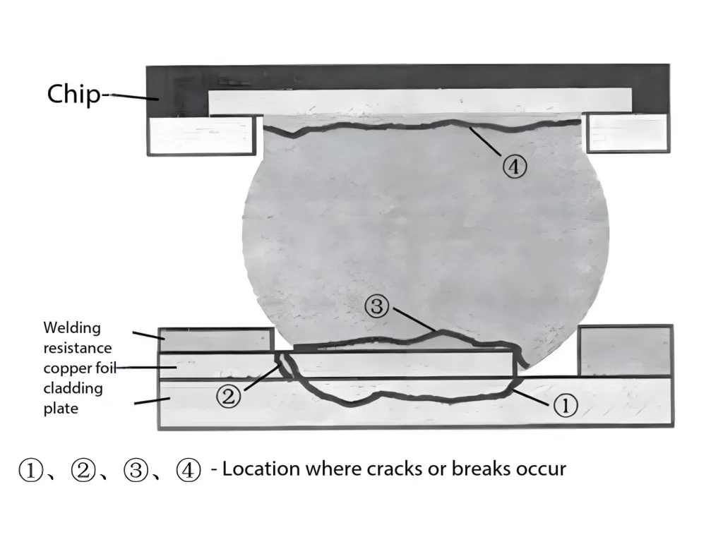
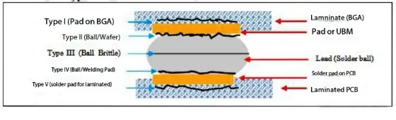
H3: 1.1 Failure Definition & Five Fracture Types
BGA pad cracking refers to the separation between IC chips and PCB pads under mechanical/thermal stress. Five fracture types are classified by location:
| Type | Failure Location | Prevalence | Primary Triggers |
|---|---|---|---|
| Type I | Chip substrate layer | 12% | Tumbling tests, mechanical shock |
| Type II | BGA pad-solder interface | 18% | Thermal cycling |
| Type III | Lead-free solder ball | 25% | Drop impact, thermal shock |
| Type IV | Solder-PCB pad joint | 28% | Reflow profile mismatch |
| Type V | Pad-substrate separation | 17% | Structural deformation, material degradation |

1.2 Stealth Nature & Destructive Impact
Traditional SMT inspection detects <5% of pad cracks due to:
-
Micro-crack sizes (5-50μm) obscured in multilayer PCBs
-
Electrical continuity often maintained despite fractures
-
Underfill masks cracks without halting propagation, requiring destructive removal during rework


2. Root Cause Analysis Across PCBA Workflow
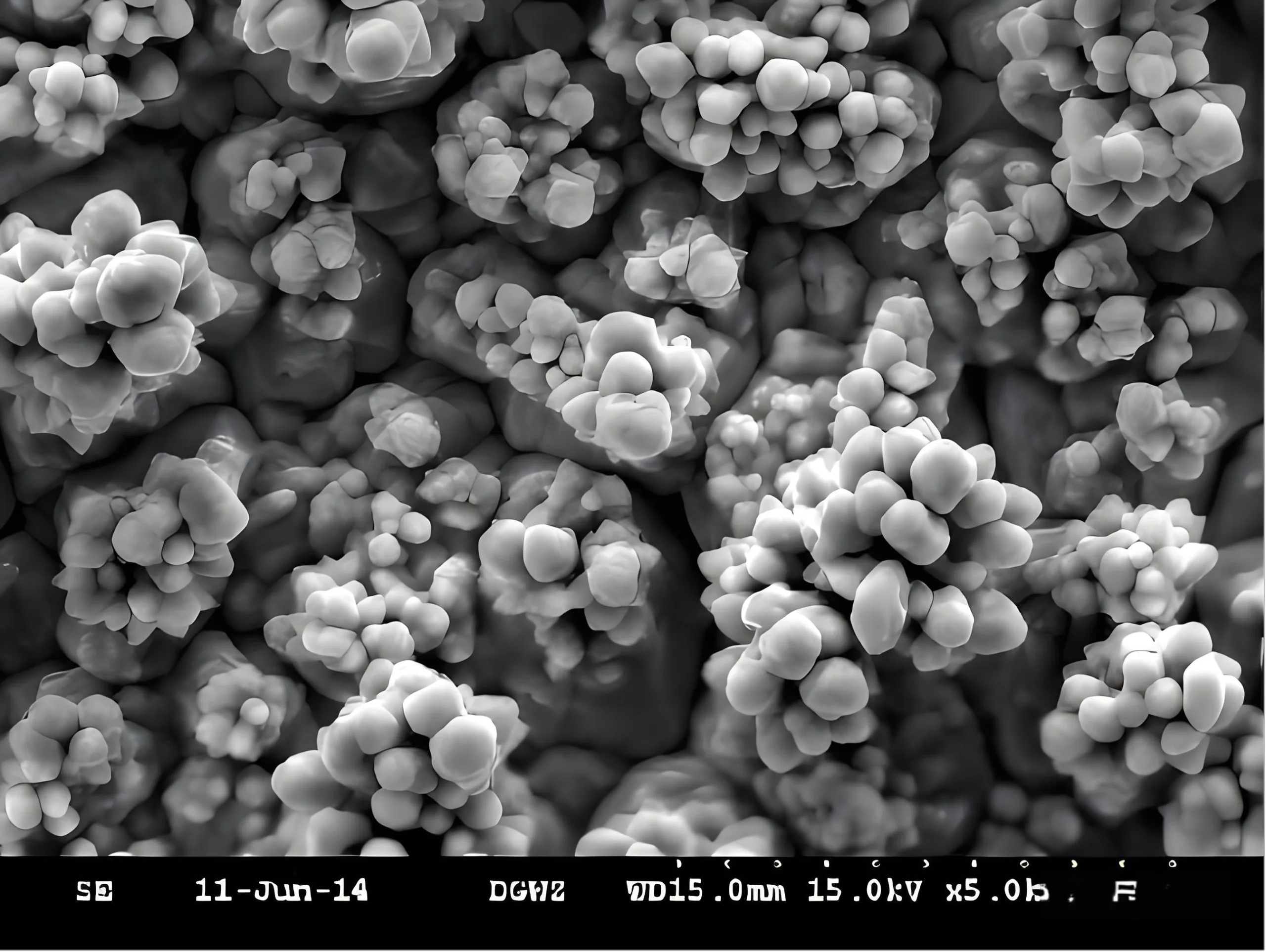
2.1 Material Origin: Copper Foil Crystal Structure Divergence
Experimental data reveals: Copper foil with specialized “grape-like” nodular structures delivers 18.5% higher adhesion than conventional crystals.

2.2 PCB Substrate Limitations: FR4’s Thermal Endurance Crisis
Lead-free soldering demands peak temperatures of 248°C (+33°C vs traditional processes). Standard FR4’s Tg of 130-140°C causes:
-
Z-axis CTE >300 ppm/°C
-
T288 delamination time <3 min (Industry requires >5 min)
Critical Formula: Thermal Stress = E × α × ΔT
Where:
σ = Thermal stress (MPa), E = Elastic modulus (GPa),
α = CTE (ppm/°C), ΔT = Temperature change (°C)
*High-CTE substrates generate 1.8× more stress at ΔT=100°C*
2.3 PCB Design Pitfalls: Overlooked Mechanical Stress
Analysis of 7,000 failed units in Russian markets shows:
-
0.80mm boards failed 3.2× more than 1.00mm boards
-
T-card slots increased PCBA cracking risk by 47%
-
Large components under BGA zones caused asymmetric thermal deformation
3. Critical PCB Process Control Breakthroughs
3.1 PCB Manufacturing Optimization Matrix
| Process | Conventional | Optimized | Improvement |
|---|---|---|---|
| Copper foil | Standard nodules | Grape-like crystals | Adhesion ↑18.5% |
| Plating thickness | 18-23μm | ≥30μm | Tensile ↑32% |
| Surface prep | Belt sanding | Micro-etch + spray | Copper loss ↓60% |
| Solder mask opening | Circular | Hexagonal | Paste flow ↑40% |
3.2 Reflow Profile Revolution
Failure root: Standard reflow spends only 12s cooling from 190°C→130°C, causing rapid contraction.
Solution: Extend dwell time above Tg by 150%, reducing thermal stress by 35%.
4. Comprehensive PCBA Solution Database
4.1 Design Innovations
-
Pad geometry: Convert peripheral pads to oval (long axis +0.1mm)
-
Stackup design: Add localized copper balance layers under BGAs
-
Clearance rule: Prohibit large components within 3mm of BGA zones
4.2 Material Upgrade Path
-
Specify FR4 with Tg ≥170°C
-
Control copper foil Rz (roughness) at 3.5-5.0μm
-
Adopt low-CTE (<2.5%) high-toughness resin systems
4.3 Process Control Redlines
-
Copper plating ≥30μm (validated)
-
OSP panel spacing >5mm (acid trapping prevention)
-
Test fixture pressure ≤7kg/cm², pin life <500k cycles
-
150-180°C reflow zone dwell ≥90 seconds
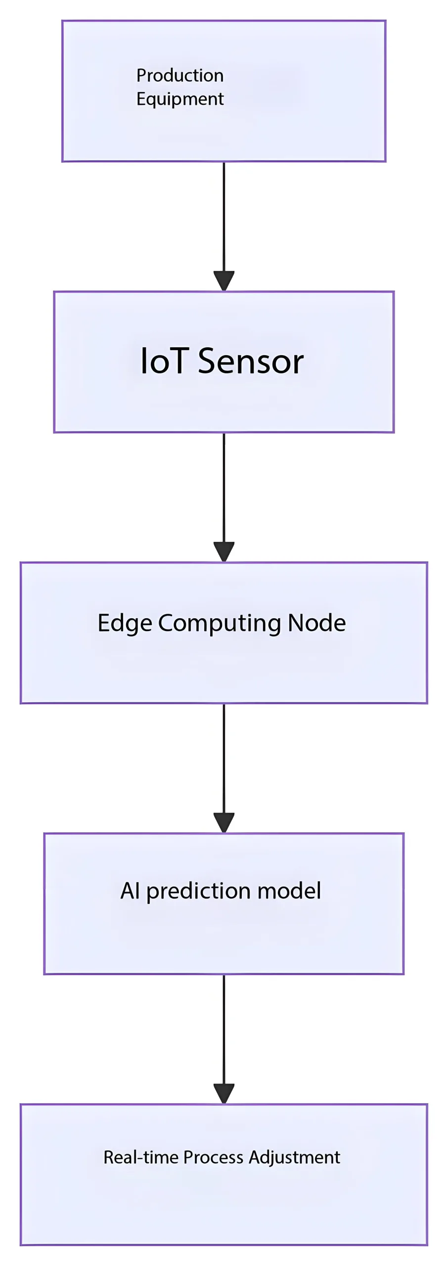
5. Future Technology Roadmap
As HDI PCBs advance toward 0.4mm thickness and BGA pads shrink below 0.2mm, breakthroughs required:
-
Nano-scale copper treatment: Magnetron-sputtered adhesion layers
-
CTE-adaptive substrates: Temperature-responsive polymer composites
-
AI process monitoring: Real-time solder joint health prediction

Conclusion: Reliability is Designed In
BGA pad cracking constitutes system-level reliability failure. Post-implementation results:
-
Tumbling test pass rate: 82% → 99.6%
-
Market return rate: ↓70%
-
Cost reduction: $1.20/board via underfill elimination
*Remember: A 0.1kgf increase in per-pad adhesion delivers exponential reliability gains. This transcends process refinement – it embodies the ultimate pursuit of zero-defect manufacturing.*
In the microscopic realm of solder pads, grape-like copper crystals weave nano-scale protective networks, while lead-free spheres perform precision dances within hexagonal mask openings. The electronics reliability revolution begins with unwavering commitment to every 0.01mm.