
Introduction to the 24 Layers Communication Backplane PCB
The 24 Layers Communication Backplane PCB is a high-performance printed circuit board designed for complex communication systems. It is engineered to provide robust connectivity and reliable signal transmission, making it ideal for advanced telecommunication applications.

What is a 24 Layers Communication Backplane PCB?
A 24 Layers Communication Backplane PCB refers to a multilayered printed circuit board that has been specifically designed with 24 layers of conductive material separated by dielectric layers. This structure allows for high-density interconnectivity while maintaining signal integrity and minimizing interference.
Design Requirements
The design requirements for a 24 Layers Communication Backplane PCB are stringent due to its application in critical communication systems. Key design considerations include:
- Material: Panasonic M6, known for its excellent thermal and electrical properties.
- Layer Count: 24 layers to accommodate complex routing needs.
- Color: Blue/White for easy identification and aesthetic appeal.
- Finished Thickness: 2.0mm to ensure structural integrity without being overly bulky.
- Copper Thickness: 1OZ to provide adequate conductivity.
- Surface Treatment: Immersion Gold to enhance solderability and corrosion resistance.
How Does It Work?
The 24 Layers Communication Backplane PCB works by using multiple layers of copper traces separated by dielectric materials. These layers are interconnected through plated through-holes (PTHs) or vias, allowing signals to travel between different layers. The immersion gold surface treatment ensures that the copper traces remain conductive and resistant to oxidation.
Applications
The primary application of the 24 Layers Communication Backplane PCB is in communication backplanes where high-speed data transmission and reliable connectivity are crucial. These PCBs are used in:
- Telecom infrastructure
- Data centers
- High-frequency communication devices
- Networking equipment
Classification
Based on its features and applications, the 24 Layers Communication Backplane PCB can be classified as a high-multilayer PCB. This classification highlights its capability to handle complex and dense circuit designs required for modern communication systems.
Material Composition
The core material used in the 24 Layers Communication Backplane PCB is Panasonic M6, a high-performance laminate material known for its excellent mechanical, thermal, and electrical properties. This material ensures that the PCB can withstand the demands of high-speed communication applications.
Performance Characteristics
The performance characteristics of the 24 Layers Communication Backplane PCB include:
- High signal integrity
- Low signal loss
- Superior thermal management
- Enhanced mechanical strength
- Reliable long-term stability
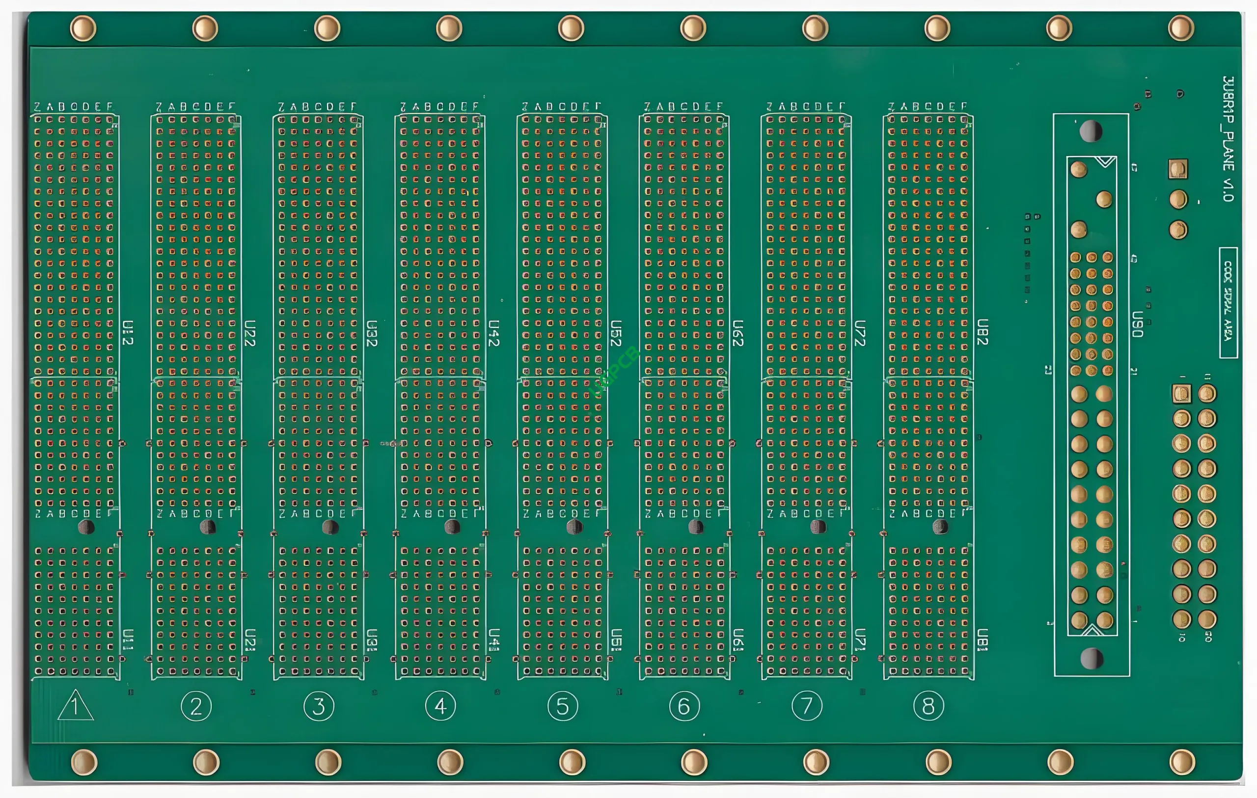
Structural Details
The structural details of the 24 Layers Communication Backplane PCB are as follows:
- Layer Count: 24 layers
- Finished Thickness: 2.0mm
- Copper Thickness: 1OZ
- Minimum Trace Width: 6mil (0.15mm)
- Minimum Space Between Traces: 6mil (0.15mm)
- Surface Treatment: Immersion Gold

Features and Benefits
The key features and benefits of the 24 Layers Communication Backplane PCB include:
- High density interconnectivity
- Excellent signal integrity
- Robust mechanical construction
- Reliable long-term performance
- Aesthetic color options (Blue/White)
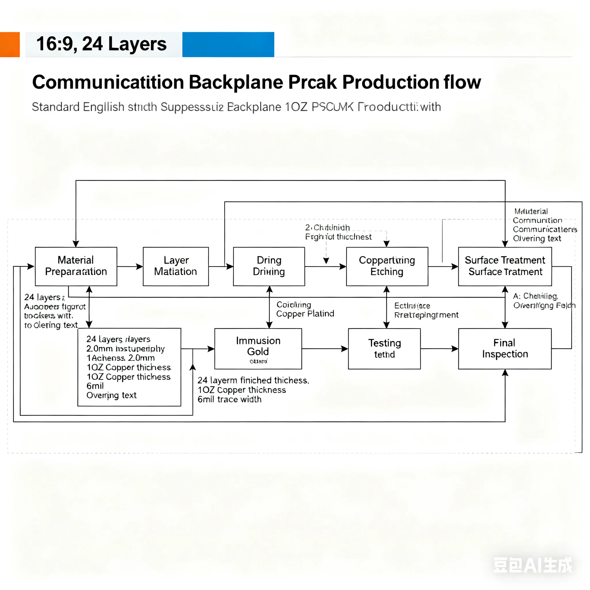
Production Process
The production process of the 24 Layers Communication Backplane PCB involves several steps, including:
- Material Selection: Choosing high-quality Panasonic M6 material.
- Layer Stacking: Arranging the 24 layers with precision.
- Etching: Removing excess copper to form the desired trace patterns.
- Plating: Applying immersion gold surface treatment.
- Assembly: Incorporating PTHs and vias for layer interconnections.
- Testing: Ensuring the PCB meets all performance specifications.
Use Cases


The 24 Layers Communication Backplane PCB is used in various scenarios, such as:
- High-speed data transmission networks
- Telecommunication infrastructure projects
- Advanced networking equipment
- Data center applications requiring high bandwidth
In summary, the 24 Layers Communication Backplane PCB is a sophisticated and reliable component designed to meet the demanding requirements of modern communication systems. Its high-density design, excellent performance characteristics, and robust construction make it an essential part of any advanced telecommunication setup.