


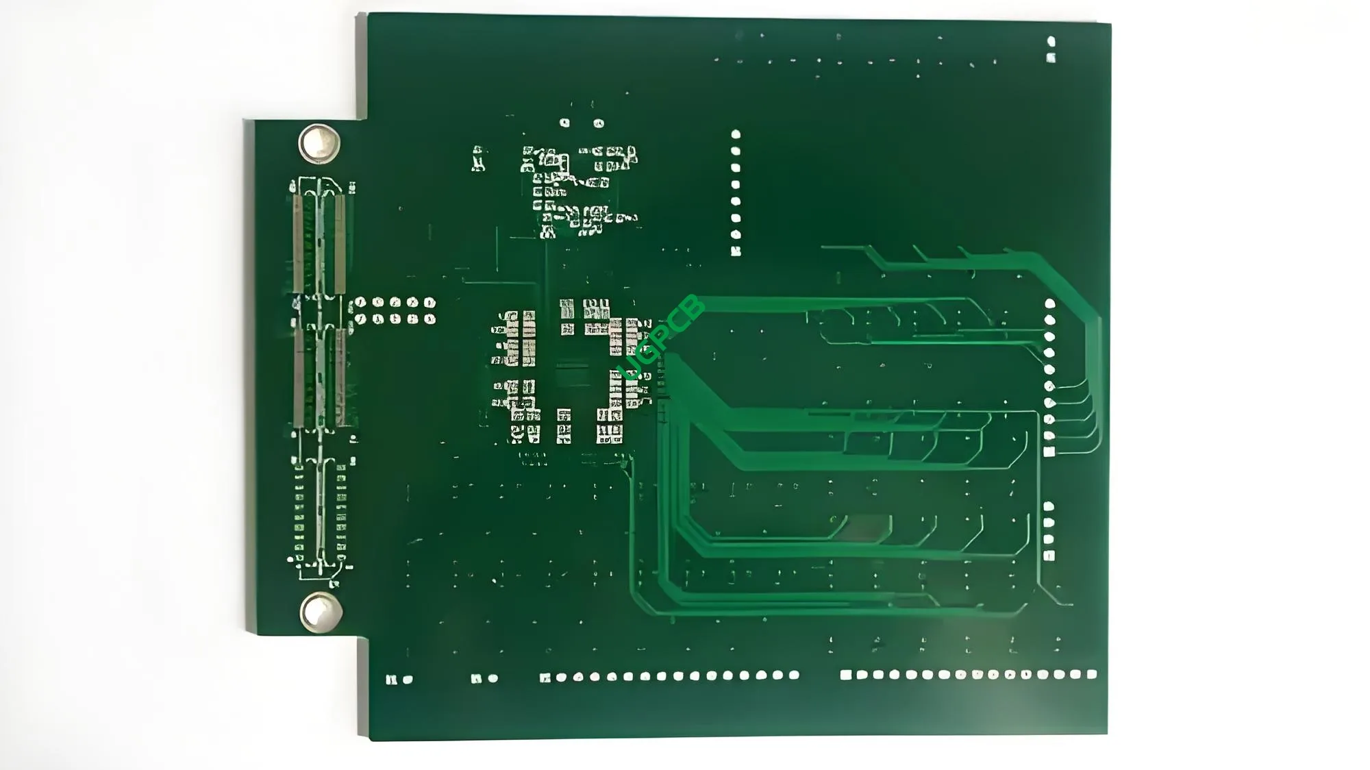
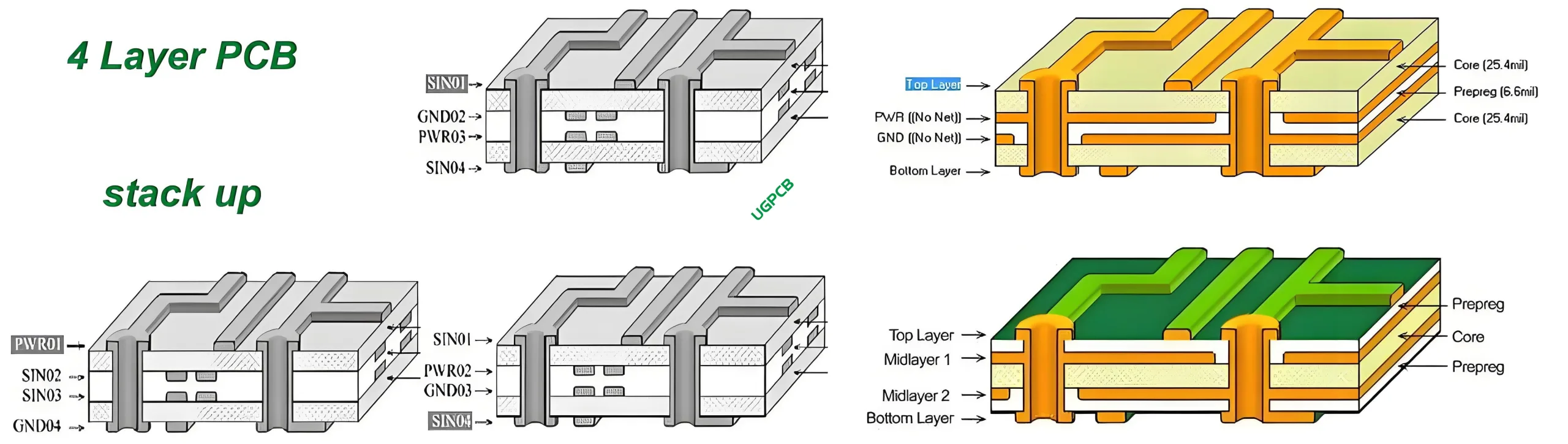
What is a 4 Layer PCB?
A 4-layer Printed Circuit Board (PCB) is an advanced electronic component that consists of four layers of conductive material, typically copper, separated by insulating layers. This multilayer structure allows for complex circuit designs with high density and improved performance.

Design Requirements
Designing a 4-layer PCB involves several key considerations:
- Material: Commonly made from FR-4, a composite material known for its excellent electrical properties and affordability.
- Layer Count: As the name suggests, it has four layers, which can handle more complex circuitry compared to single or double-sided boards.
- Copper Thickness: Can range from 0.5OZ to 6OZ, depending on the application’s power requirements.
- Surface Treatment: Options include immersion gold, OSP (Organic Solderability Preservative), and lead-free HASL (Heat Activated Solder Leveling), each offering different levels of solderability and protection.
- Trace and Space: Minimum trace and space are typically set at 3mil (0.075mm), allowing for fine details in the circuit design.
How Does it Work?
The 4-layer PCB functions by providing a platform where electronic components can be mounted and interconnected using conductive pathways etched into the copper layers. These pathways are separated by insulating layers, preventing electrical shorts while allowing signals to pass through via plated through-holes or vias.
Applications
Due to their complexity and reliability, 4-layer PCBs are widely used in various consumer electronics including:
- Smartphones
- Tablets
- Laptops
- Gaming consoles
- High-end audio equipment


Classification
4-layer PCBs can be classified based on several factors:
- By Material: Most commonly made from FR-4 due to its balance of cost, strength, and electrical properties.
- By Copper Thickness: Varies from lightweight (0.5OZ) to heavyweight (6OZ) depending on the application’s needs.
- By Surface Treatment: Options include immersion gold, OSP, and lead-free HASL, each offering different levels of protection and solderability.
Materials Used
The primary materials used in manufacturing 4-layer PCBs include:
- FR-4: A glass-reinforced epoxy laminate that provides excellent mechanical strength and thermal stability.
- Copper: Used for the conductive layers, with thickness varying based on design requirements.
- Solder Mask: Typically green, white, red, or black, it protects the copper traces from oxidation and accidental short circuits.
- Surface Treatments: Such as immersion gold, OSP, or lead-free HASL, which improve solderability and protect against corrosion.
Performance Characteristics
Key performance attributes of a 4-layer PCB include:
- High Density: Allows for more components to be packed into a smaller area.
- Reliability: The use of multiple layers reduces the risk of electrical shorts and improves signal integrity.
- Signal Integrity: Improved due to shorter signal paths and reduced crosstalk.
Structural Composition
Structurally, a 4-layer PCB comprises:
- Conductive Layers: Made of copper, etched into the desired circuit patterns.
- Insulating Layers: Prevent electrical shorts between conductive layers.
- Plated Through-Hole Vias: Facilitate connections between different layers.

Distinctive Features
Some notable features of a 4-layer PCB are:
- Fine Pitch: Allows for high-density interconnects, making it ideal for compact devices.
- Robustness: The use of multiple layers provides a strong mechanical bond between the board and components.
- Versatility: Suitable for a wide range of applications due to customizable layer counts and material choices.
Production Process
The manufacturing process of a 4-layer PCB involves several steps:
- Design and Layout: Using specialized software to create the circuit pattern.
- Material Preparation: Cutting base materials to size and cleaning surfaces.
- Lamination: Stacking and bonding individual layers under heat and pressure.
- Etching: Removing excess copper to form the desired circuit paths.
- Plating: Adding a thin layer of metal to vias and exposed copper areas.
- Solder Mask Application: Applying the green, white, red, or black coating to protect traces.
- Surface Treatment: Applying immersion gold, OSP, or lead-free HASL for solderability.
- Final Inspection: Ensuring quality and functionality before shipment.
Use Cases
Common scenarios where a 4-layer PCB might be employed include:
- High-density interconnect applications in mobile devices.
- Advanced communication systems requiring low signal loss.
- Portable medical instruments needing reliable performance in harsh environments.
- Automotive electronics demanding robustness and longevity.
In summary, the 4-layer PCB represents a significant advancement in printed circuit board technology, offering unparalleled complexity and performance for modern electronic applications. Its design flexibility combined with superior signal integrity and durability makes it an essential component in the development of next-generation consumer electronics and beyond.