

6L 1+N+1 HDI Product Overview
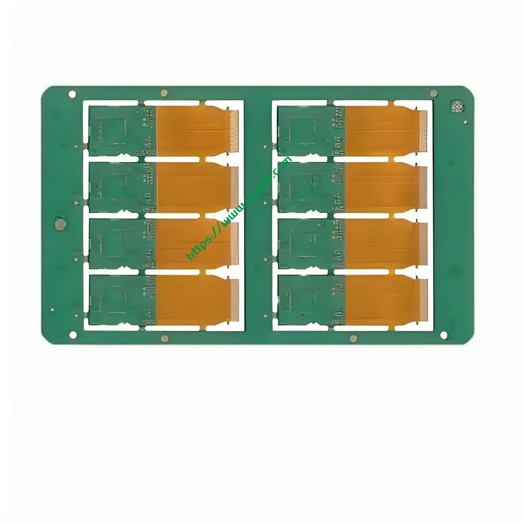
The 6L 1+N+1 HDI product is a high-density interconnect (HDI) printed circuit board (PCB) designed for advanced electronic applications. This PCB features six layers, including one core layer surrounded by alternating layers of conductive and non-conductive materials, with additional conductive layers on the outermost sides. The use of FR-4 material ensures durability and excellent electrical performance.


Key Features and Design Requirements
- Material: FR-4, known for its flame-resistant properties and high mechanical strength.
- Layers: Six layers arranged in a 1+N+1 configuration, providing flexibility in design and functionality.
- Color: Available in green or white to suit different aesthetic preferences or identification needs.
- Finished Thickness: A standard thickness of 0.8mm, ensuring compatibility with various device casings.
- Copper Thickness: Inner layers feature 1oz copper, while outer layers are thicker at 0.5oz for enhanced conductivity and durability.
- Surface Treatment: Immersion gold combined with OSP (Organic Solderability Preservative) PCB finish for improved solderability and corrosion resistance.
- Min Trace / Space: Capable of handling trace widths and spaces as fine as 3mil/3mil, ideal for compact designs.
- Min Hole: Supports both mechanical holes down to 0.2mm and laser drilled holes as small as 0.1mm, enabling intricate component placement.
Working Principle and Applications
The working principle behind the 6L 1+N+1 HDI PCB revolves around maximizing connectivity within a limited space through strategic layering and advanced manufacturing techniques. By incorporating multiple layers of conductive pathways separated by dielectric materials, this PCB can handle complex circuit designs with minimal signal interference and crosstalk. Its high-density layout is particularly advantageous for portable electronic devices where miniaturization and functionality are paramount.
Classification and Use Cases
As a high-density interconnect PCB, the 6L 1+N+1 HDI falls under the category of advanced PCBs tailored for demanding electronic applications. It’s widely used in:
- Portable electronic devices such as smartphones, tablets, and wearables, where space optimization is crucial.
- High-performance computing components requiring efficient heat dissipation and signal integrity.
- Aerospace and military equipment demanding reliability under extreme conditions.
Production Process and Quality Control
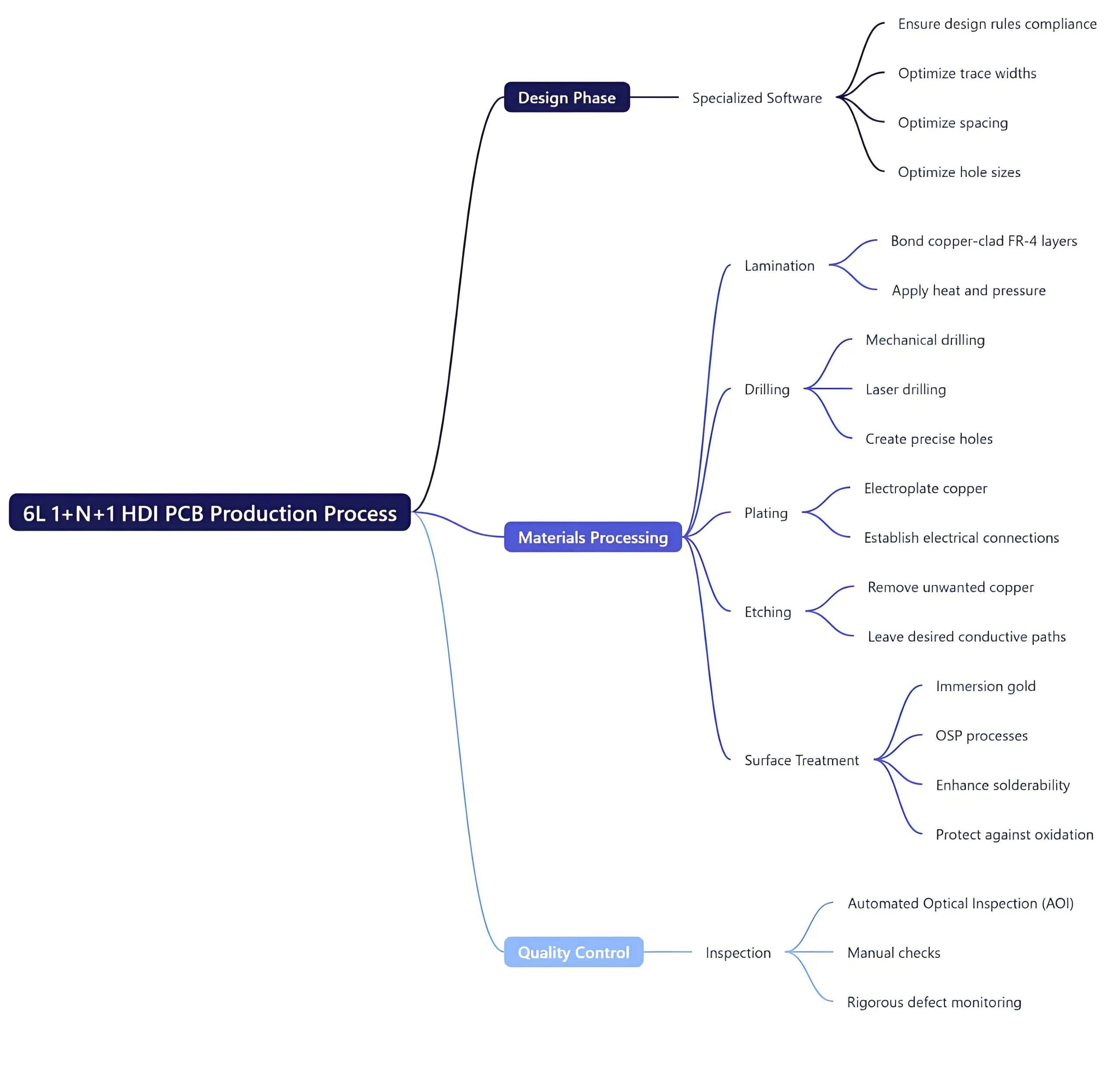

The production process begins with careful design using specialized software to ensure all design rules are met. This includes optimizing trace widths, spacing, and hole sizes for manufacturability. Next, the raw materials undergo several stages of processing:
- Lamination: Layers of copper-clad FR-4 are bonded together under heat and pressure.
- Drilling: Mechanical and laser drilling create precise holes for component leads and interconnections.
- Plating: Copper is electroplated onto the walls of the drilled holes to establish electrical connections between layers.
- Etching: Unwanted copper is removed, leaving only the desired conductive paths.
- Surface Treatment: Immersion gold and OSP processes enhance solderability and protect against oxidation.
- Inspection: Each PCB undergoes rigorous inspection for defects using automated optical inspection (AOI) systems and manual checks.
Conclusion
The 6L 1+N+1 HDI PCB stands out as a versatile solution for modern electronic design challenges, offering exceptional density, reliability, and performance. Its sophisticated construction and meticulous manufacturing process make it an ideal choice for applications requiring compact size without compromising on functionality or quality. Whether it’s for consumer electronics, high-tech gadgets, or critical industrial systems, this PCB delivers unparalleled connectivity in a compact form factor.