


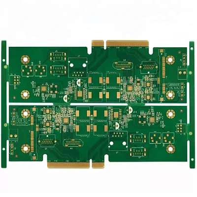
Overview of 6 Layer Golden Finger PCB
The 6 Layer Golden Finger PCB is a high-precision, multi-layered printed circuit board designed for advanced electronic applications. This product combines multiple layers of conductive traces and insulating materials to provide exceptional performance and reliability in various electronic devices.
Definition
A 6 Layer Golden Finger PCB is a type of multi-layer printed circuit board (PCB) that features six individual layers of conductive material, separated by insulating layers. The term “Golden Finger” refers to the specific surface treatment applied to the edges of the board, which involves immersion gold and additional gold plating on the contact fingers.
Design Requirements
When designing a 6 Layer Golden Finger PCB, several key requirements must be considered:
- Material Quality: High-quality FR4 material is essential for durability and performance.
- Layer Configuration: Six layers are needed to accommodate complex circuitry and signal routing.
- Copper Thickness: A standard copper thickness of 1OZ ensures adequate conductivity.
- Surface Treatment: Immersion gold with additional gold finger plating enhances connectivity and corrosion resistance.
- Trace/Space Dimensions: A minimum trace/space of 4mil/4mil is required for precise circuit patterns.
- Special Processes: The gold finger process with a thickness of 0.1um is critical for reliable edge connections.
Working Principle
The 6 Layer Golden Finger PCB operates based on the principles of electrical conductivity and insulation. Conductive traces on different layers create pathways for electrical signals, while insulating layers prevent unwanted interactions between these signals. The gold finger edges facilitate easy insertion into connectors, ensuring stable and reliable connections.
Applications
This type of PCB is widely used in applications that require high precision and reliability, such as:
- High-speed digital circuits
- Telecommunications equipment
- Advanced computing systems
- Automotive electronics
- Medical devices
Classification
6 Layer Golden Finger PCBs can be classified based on their intended use, such as:
- Signal Processing Boards: For handling high-frequency signals in communication devices.
- Power Distribution Boards: To manage power supply in complex electronic systems.
- Control Boards: For controlling and managing various functions in electronic devices.
Materials
The primary materials used in the construction of a 6 Layer Golden Finger PCB include:
- Base Material: FR4, a flame-retardant fiberglass material known for its excellent dielectric properties and mechanical strength.
- Conductive Material: Copper, used for the conductive traces.
- Surface Treatment: Immersion gold and additional gold plating for the gold fingers.
Performance
The performance of a 6 Layer Golden Finger PCB is characterized by:
- High Signal Integrity: Due to precise trace/space dimensions and quality materials.
- Reliable Connectivity: Ensured by the gold finger surface treatment.
- Durability: Enhanced by the robust FR4 base material and immersion gold finish.
- Electrical Efficiency: Minimized signal loss and interference due to optimized layer configuration.
Structure
The structure of a 6 Layer Golden Finger PCB consists of:
- Six Layers of Conductive Material: Alternating with insulating layers.
- Gold Finger Edges: Plated with a thin layer of gold for enhanced connectivity.
- Protective Layers: Including solder mask and silkscreen for protection and identification.
Features
Key features of the 6 Layer Golden Finger PCB include:
- Advanced Surface Treatment: Immersion gold plus gold finger for superior connection quality.
- High Precision: With a minimum trace/space of 4mil/4mil.
- Customizable Color Options: Available in green or white.
- Standard Thickness: With a finished thickness of 1.6mm.
Production Process
The production process for a 6 Layer Golden Finger PCB involves several steps:
- Material Preparation: Selecting and preparing FR4 sheets and copper foil.
- Layer Stacking: Alternating layers of copper and insulating materials.
- Etching: Removing excess copper to form the desired circuit pattern.
- Plating: Applying immersion gold and additional gold finger plating.
- Lamination: Combining the layers under heat and pressure.
- Drilling: Creating holes for through-hole components and vias.
- Solder Mask Application: Protecting the circuit from solder bridges and environmental factors.
- Silkscreen Printing: Adding text and symbols for component placement and identification.
- Quality Control: Ensuring the PCB meets all design specifications and standards.
Use Scenarios
The 6 Layer Golden Finger PCB is ideal for scenarios where:
- High signal integrity is crucial.
- Reliable and durable connections are required.
- Space constraints necessitate a compact and efficient design.
- Advanced surface treatment is needed for enhanced performance.