
Introduction to 4 Layers Industrial Control PCBA
Overview
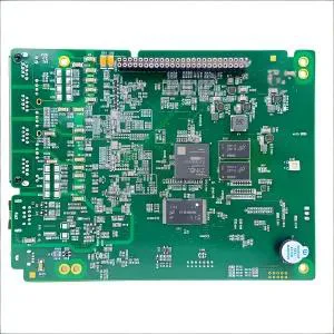
The 4 Layers Industrial Control PCBA is a sophisticated printed circuit board assembly designed for industrial control applications. It features four layers of conductive material, which allows for complex circuitry and high-density component placement. This PCBA is essential for various industrial automation and control systems due to its reliability and performance.

Definition
A 4 Layers Industrial Control PCBA refers to a multi-layer printed circuit board assembly that incorporates four layers of copper traces, separated by dielectric layers. This design enables more compact and efficient circuit designs suitable for industrial environments.
Working Principle
The working principle of a 4 Layers Industrial Control PCBA involves the use of multiple layers of conductive copper traces embedded within non-conductive substrate layers. These layers are interconnected through vias (plated-through holes) to allow electrical signals to travel between different layers. The surface mount technology (SMT) and through-hole technology (THT) components are soldered onto the PCB, creating a functional circuit.
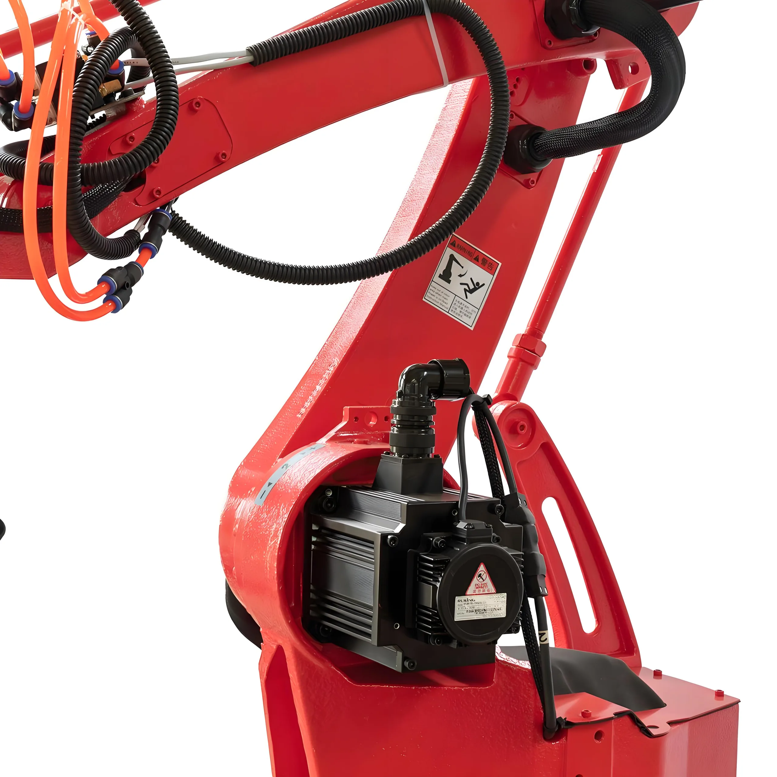
Applications
This type of PCBA is widely used in industrial control systems, including:
- Automation equipment
- Robotics
- Machine control units
- Sensor interfaces
- Power distribution boards

Classification
PCBAs can be classified based on several criteria:
- By number of layers: Single-sided, double-sided, multi-layer (including 4 layers)
- By type of components: Through-hole, surface mount, or a combination of both
- By industry standards: RoHS compliant, lead-free, etc.
Materials
The primary materials used in the construction of a 4 Layers Industrial Control PCBA include:
- Copper foil for the conductive layers
- Fiberglass or composite materials for the dielectric layers
- Lead-free HASL (Heat Sink Assembly Level) surface finish
- Green solder mask for protection and insulation
Performance
The performance of this PCBA is characterized by:
- High thermal conductivity due to the copper layers
- Low signal loss and high signal integrity
- Resistance to environmental factors such as humidity, temperature variations, and mechanical stress
- Compliance with RoHS and lead-free assembly standards
Structure
The structure of a 4 Layers Industrial Control PCBA typically includes:
- Four layers of copper traces separated by dielectric layers
- Vias (plated-through holes) for inter-layer connectivity
- Surface mount and through-hole components soldered onto the board
- A green solder mask covering the top layer for protection and identification
Features
Key features of this PCBA include:
- High density and compact design suitable for space-constrained applications
- Superior thermal management capabilities
- Enhanced durability and longevity in harsh industrial environments
- Compatibility with a wide range of electronic components
Production Process
The production process of a 4 Layers Industrial Control PCBA involves several steps:
- Design: Using specialized software to create the circuit layout and component placement.
- Material Preparation: Selecting and preparing the copper foil, dielectric layers, and other materials.
- Layer Stacking: Stacking the layers of copper and dielectric materials.
- Via Drilling: Drilling holes through the stacked layers for vias.
- Plating: Plating the vias with copper to ensure electrical connectivity.
- Etching: Removing excess copper to form the desired circuit pattern.
- Component Placement: Soldering surface mount and through-hole components onto the PCB.
- Testing: Conducting rigorous testing to ensure functionality and compliance with standards.
- Final Inspection: Ensuring the PCBA meets all quality and performance criteria.


Use Cases
Common use cases for the 4 Layers Industrial Control PCBA include:
- Industrial automation systems where high reliability and performance are crucial
- Robotic arms and machinery requiring precise control
- Manufacturing plants with demanding environmental conditions
- Power distribution and control panels in heavy industries
Conclusion
The 4 Layers Industrial Control PCBA is an advanced and reliable solution for various industrial control applications. Its multi-layer design, high-performance materials, and compliance with industry standards make it an ideal choice for engineers and manufacturers seeking robust and efficient electronic solutions.