


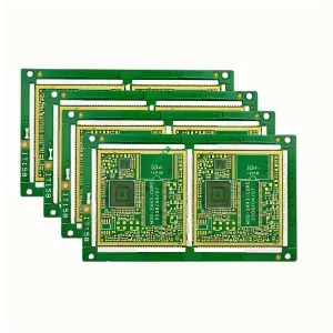
Overview of Multilayer Vehicle WiFi Module PCB
The multilayer vehicle WiFi module PCB is a specialized product designed to meet the stringent requirements of automotive WiFi and Bluetooth applications. This type of PCB offers high precision, reliability, and performance, making it an ideal choice for various in-vehicle communication systems.

Definition
A multilayer vehicle WiFi module PCB is a printed circuit board specifically designed to support the functions of a WiFi or Bluetooth module in automotive applications. It consists of multiple layers of conductive and insulating materials, providing complex electrical pathways and connections essential for the operation of the module.
Design Requirements
When designing a multilayer vehicle WiFi module PCB, several key requirements must be met:
- Material Quality: High-quality FR4 material is essential for durability and signal integrity.
- Layer Configuration: A 6-layer design is standard, allowing for complex circuitry and signal routing.
- Copper Thickness: A copper thickness of 1OZ ensures adequate conductivity.
- Surface Treatment: Immersion gold surface treatment enhances connectivity and corrosion resistance.
- Trace/Space Dimensions: Minimum trace and space dimensions of 3mil (0.75mm) are required for precise circuit patterns.
- Special Features: Half-hole PCB design is often incorporated for specific component placement and soldering requirements.
Working Principle
The multilayer vehicle WiFi module PCB operates based on the principles of electrical conductivity and insulation. Conductive layers form the pathways for electrical signals, while insulating layers prevent unwanted interactions between these signals. The immersion gold surface treatment provides excellent connectivity and protects against environmental factors.
Applications
This type of PCB is primarily used in automotive WiFi and Bluetooth modules, which are crucial components in various in-vehicle communication and entertainment systems. These include:
- In-vehicle WiFi hotspots
- Bluetooth connectivity for hands-free calling and audio streaming
- Telematics and remote diagnostics systems
- Infotainment systems
Classification
Multilayer vehicle WiFi module PCBs can be classified based on their specific features and intended use, such as:
- Communication Boards: For handling wireless communication signals in vehicles.
- Control Boards: For managing and controlling various functions in electronic systems.
- Power Distribution Boards: To manage power supply in complex electronic systems.
Materials
The primary materials used in the construction of a multilayer vehicle WiFi module PCB include:
- Base Material: FR4, a flame-retardant fiberglass material known for its excellent dielectric properties and mechanical strength.
- Conductive Material: Copper, used for the conductive traces.
- Surface Treatment: Immersion gold, which enhances connectivity and provides corrosion resistance.
Performance
The performance of a multilayer vehicle WiFi module PCB is characterized by:
- High Signal Integrity: Due to precise trace/space dimensions and quality materials.
- Reliable Connectivity: Ensured by the immersion gold surface treatment.
- Durability: Enhanced by the robust FR4 base material.
- Electrical Efficiency: Minimized signal loss and interference due to optimized layer configuration.
Structure
The structure of a multilayer vehicle WiFi module PCB consists of:
- Six Layers of Conductive Material: Alternating with insulating layers.
- Immersion Gold Surface Treatment: For enhanced connectivity and protection.
- Half-Hole Design: For specific component placement and soldering requirements.
Features
Key features of the multilayer vehicle WiFi module PCB include:
- Advanced Surface Treatment: Immersion gold for superior connection quality.
- High Precision: With minimum trace and space dimensions of 3mil (0.75mm).
- Customizable Color Options: Available in green or white.
- Standard Thickness: With a finished thickness of 1.0mm.
Production Process
The production process for a multilayer vehicle WiFi module PCB involves several steps:
- Material Preparation: Selecting and preparing FR4 sheets and copper foil.
- Layer Stacking: Alternating layers of copper and insulating materials.
- Etching: Removing excess copper to form the desired circuit pattern.
- Plating: Applying immersion gold surface treatment.
- Lamination: Combining the layers under heat and pressure.
- Drilling: Creating holes for through-hole components and vias.
- Solder Mask Application: Protecting the circuit from solder bridges and environmental factors.
- Silkscreen Printing: Adding text and symbols for component placement and identification.
- Quality Control: Ensuring the PCB meets all design specifications and standards.
Use Scenarios

The multilayer vehicle WiFi module PCB is ideal for scenarios where:
- High signal integrity is crucial.
- Reliable and durable connections are required.
- Space constraints necessitate a compact and efficient design.
- Advanced surface treatment is needed for enhanced performance.