
Na indústria de fabricação eletrônica em rápida evolução, SMT defeitos de lápide (comumente referido como efeito de Manhattan ou defeitos de lápide) continuam a ser um gargalo crítico que limita as melhorias em PCB e PCBA rendimento de primeira passagem. À medida que os avanços impulsionados pela IA impulsionam atualizações abrangentes na tecnologia de PCB, inovações em materiais, processos, e arquiteturas estão inaugurando um novo ciclo da indústria. A ampla adoção de componentes de chips em miniatura, como 0402 (01005) pacotes, levou ao ressurgimento do fenômeno Manhattan com taxas de ocorrência mais altas, emergindo como um desafio inevitável na fabricação de alta qualidade. Este artigo fornece uma análise aprofundada das causas da lápide com base em Padrões IPC e modelos mecânicos, ao mesmo tempo que fornece uma estratégia de prevenção abrangente que abrange o design, Materiais, e otimização de processos.
O fenômeno de Manhattan: O assassino invisível na soldagem SMT
O fenômeno Manhattan é um defeito comum na soldagem por refluxo SMT, onde uma extremidade de um componente do chip se destaca da almofada, girando verticalmente em um ângulo (normalmente 30°–90°), assemelhando-se a um arranha-céu ou lápide - daí seu nome. Este defeito não só compromete a conectividade elétrica, mas também pode levar a curtos-circuitos, juntas frias, e outras questões, diminuindo severamente a confiabilidade do produto.
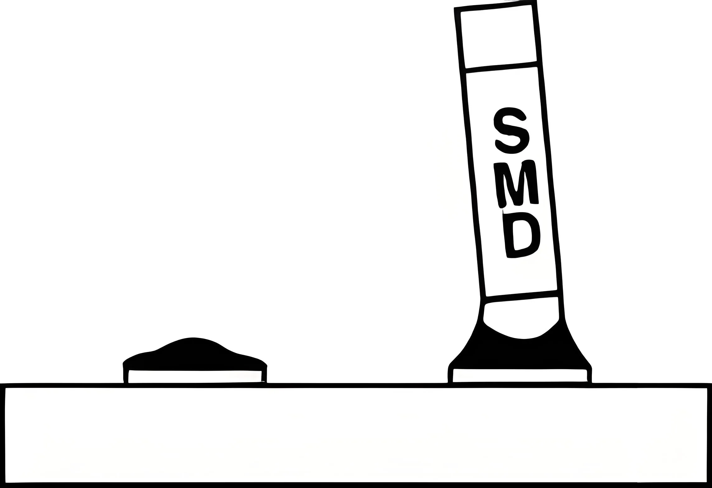
O problema central decorre de um desequilíbrio de torque causado por forças desiguais nas extremidades dos componentes. Quando a pasta de solda em uma extremidade derrete primeiro e gera forças de umedecimento, enquanto a extremidade oposta permanece não derretida, o diferencial de tensão superficial puxa o componente para cima, formando uma lápide. De acordo com modelos mecânicos, a marcação para exclusão ocorre quando o fator de equilíbrio Eb excede 1.
Mecanismo Mecânico e Parâmetros Chave do Fenômeno Manhattan
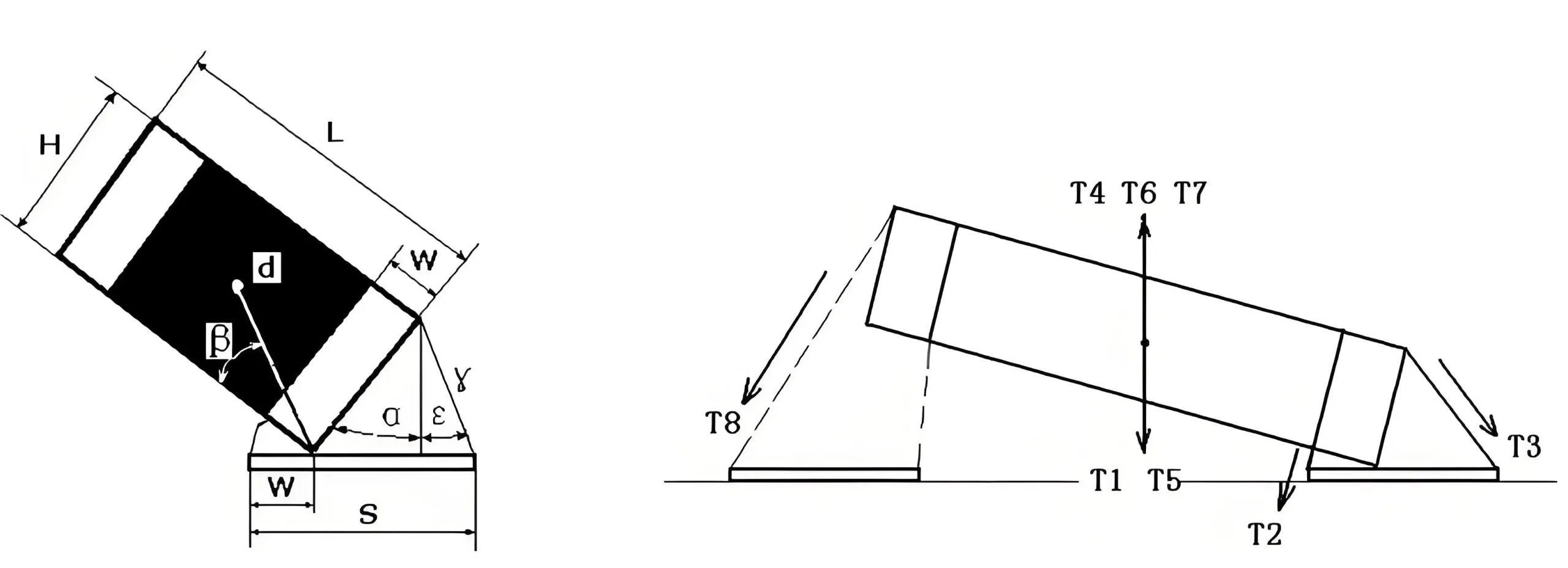
Análise do modelo de força
As forças que atuam em um componente durante a soldagem por refluxo são complexas e incluem principalmente os seguintes momentos:
-
Momentos de resistência:
-
T1 = Mgdcos(a+b) (gravidade componente)
-
T2 = γωcos(a/2) (tensão superficial da solda fundida na parte inferior do componente)
-
T5 = Adcos(a+b) (força adesiva da pasta de solda)
-
-
Momentos de condução:
-
T3 = γHsin(a+d) (tensão superficial no filete final do componente)
-
T6 = Mvdcos(a+b) (força induzida pela vibração do transportador)
-
T7 = Lhρgdcos(a+b) (flutuabilidade máxima da geração de gás na pasta de solda)
-
Fator de equilíbrio Eb = (T3 + T6 + T7) / (T1 + T2 + T5)
Quando Eb > 1, momentos de condução superam momentos de resistência, inevitavelmente causando o efeito Manhattan.
Papel crítico da tensão superficial
A pasta de solda fundida minimiza a área de superfície de acordo com o princípio da minimização de energia. Sua tensão superficial é definida como σ = (Fs – Fv) · n1, onde Fs é energia livre de superfície, Fv é energia livre de volume, e n1 é o número de moléculas por unidade de área.
Da equação de Laplace, a pressão adicional na superfície do líquido é: Pad = 2σH, onde H = ½(1/R1 + 1/R2). As diferenças na curvatura da solda fundida nas extremidades dos componentes criam uma pressão adicional desigual, levando a uma tensão superficial não uniforme e iniciando a lápide.
Análise de 16 Principais fatores que influenciam o fenômeno de Manhattan
Projeto de PCB e fatores de materiais
-
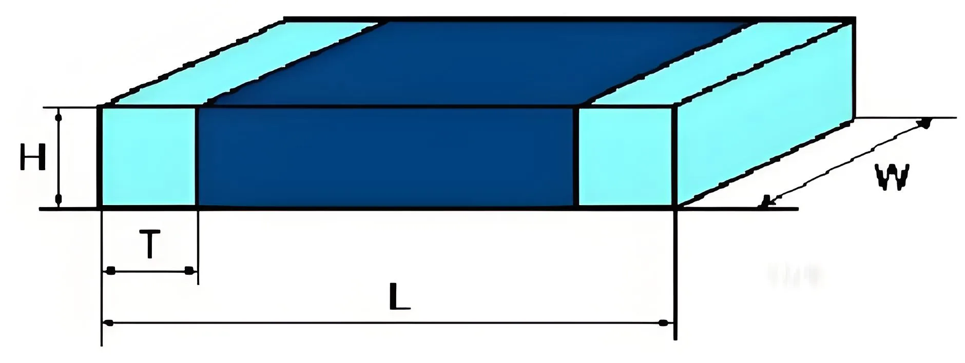
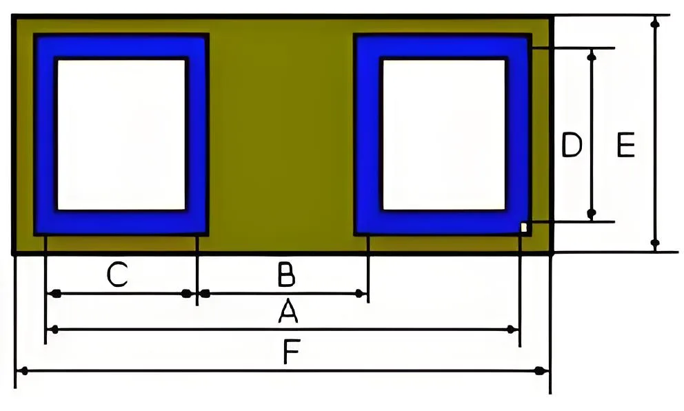
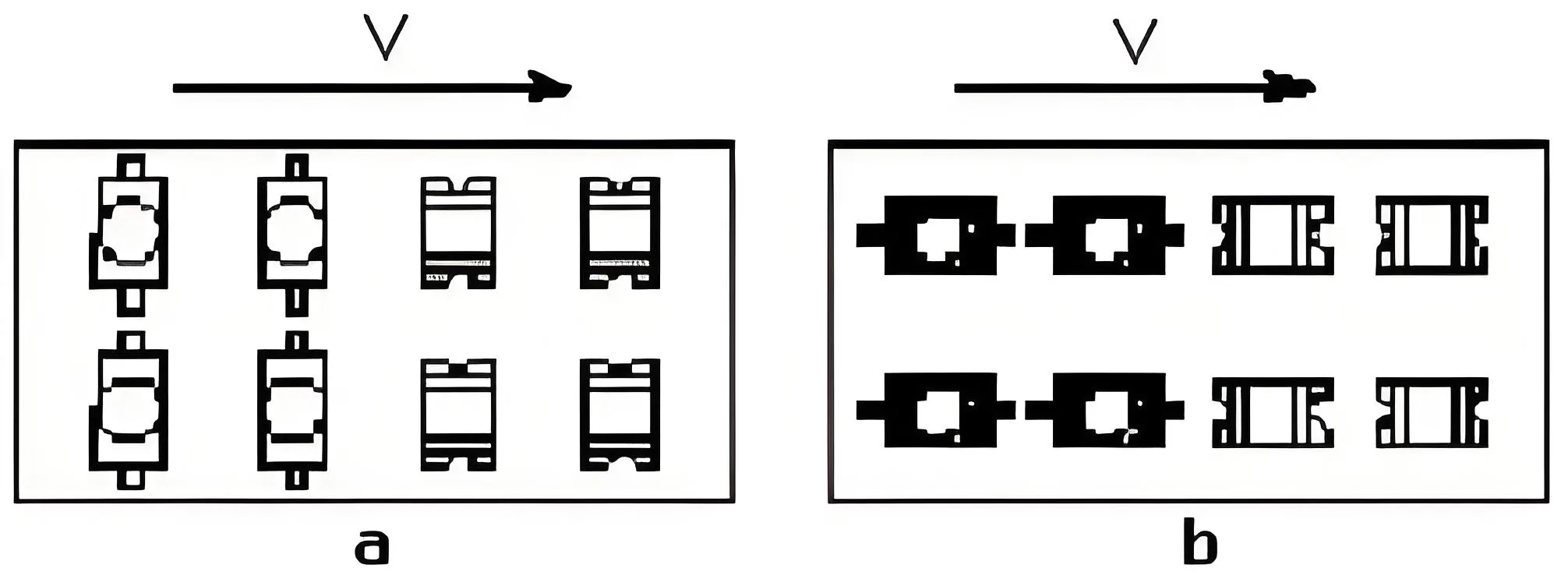
Design de almofada assimétrica: A não conformidade com os padrões IPC-7351/IPC-SM-782 resulta em capacidade térmica irregular. As dimensões recomendadas da almofada devem aderir estritamente aos padrões; por exemplo, para 0402 componentes, comprimento da almofada A = 1,50 mm, largura B = 0,50 mm.
-
Incompatibilidade entre o espaçamento do componente e do PCB: Causa forças de umedecimento desequilibradas.
-
Variação da capacidade térmica nas almofadas: Almofadas maiores têm maior capacidade térmica, aquecer mais devagar, e atrasar o derretimento da solda.
-
Substrato PCB Condutividade térmica: A incidência é maior com substratos de epóxi de papel (≥8%), seguido de epóxi de vidro (≈5%), e mais baixo com cerâmica de alumina (≤2%).
-
Volume de pasta de solda assimétrica: Erros de impressão ou espessura inconsistente levam a diferenças de capacidade térmica.
-
Contaminação ou oxidação da camada de níquel ENIG: Resulta em baixa molhabilidade e tempo de umedecimento prolongado.
-
Revestimento fino HASL: Forma camadas IMC inferiores, força de umedecimento insuficiente.
-
Variação da atividade da pasta de solda: Má uniformidade de fluxo ou pré-volatilização excessiva.
Fatores de processos e equipamentos SMT
-
Aquecimento irregular nas extremidades dos componentes: Variação lateral da temperatura do forno de refluxo ΔT > ±2°C faz com que uma extremidade derreta primeiro.
-
Posicionamento de componentes desalinhados: >25% discrepância na sobreposição do componente ao PCB causa transferência de calor desigual.
-
Marcação para exclusão devido à colocação sem contato: Componentes que não entram em contato total com a pasta de solda prejudicam a condução de calor.
-
Roubo de solda ou bolhas de vias adjacentes: Reduz o volume da pasta de solda, alterando a capacidade térmica.
-
Efeito Parede de Vento em Fornos de Refluxo: A frequência incorreta do ventilador cria diferenças localizadas de temperatura.
-
Pré-aquecimento insuficiente: Temperatura ou duração inadequada de pré-aquecimento aumenta ΔT.
-
Orientação inadequada de componentes: Não garante a entrada simultânea de ambas as extremidades na zona de refluxo.
-
Uso incorreto da atmosfera N2: A prevenção excessiva da oxidação acelera a umectação inicial, reduzindo a janela de ajuste ΔT.
Estratégia abrangente de prevenção e solução para o fenômeno Manhattan
Otimizando o Design do Pad – Aderindo aos padrões IPC
A estrita conformidade com os padrões IPC-7351B para design de almofadas é fundamental. Dimensões recomendadas da almofada (em mm) são:
| Tipo de componente | Comprimento da almofada (UM) | Largura da almofada (B) | Espaçamento entre almofadas (C) | Comprimento da almofada sob o componente (D) |
|---|---|---|---|---|
| 0201 | 0.75 | 0.23 | 0.23 | 0.31 |
| 0402 | 1.50 | 0.50 | 0.50 | 0.60 |
| 0603 | 2.10 | 0.90 | 0.60 | 0.90 |
| 0805 | 2.60 | 1.20 | 0.70 | 1.30 |
Garanta a simetria da almofada; o comprimento da almofada do subcomponente deve exceder a largura da extremidade metálica para melhorar o momento anti-marcação T2.
Refinando os Processos de Impressão e Colocação
-
Controle de impressão de pasta de solda: Utilize 3D SPI para inspecionar a espessura e a área da pasta, garantindo diferença de volume entre as extremidades <10%. Mantenha a espessura em 100–130μm, com limpeza regular do estêncil e teste de tensão.
-
Aprimoramento da precisão do posicionamento: Utilize posicionadores de alta velocidade da série Siemens SX com calibração a laser 3D para precisão de posicionamento de ±25 μm, garantindo contato uniforme entre as extremidades dos componentes e a pasta de solda.
-
Otimização da orientação de componentes: Projeto com eixo longo do componente perpendicular à linha limite de refluxo, permitindo a entrada simultânea de ambas as extremidades na zona de fusão para fusão sincronizada.
Controle preciso de perfil de solda por refluxo
-
Pré-aquecimento adequado: Pré-aqueça a 150–180°C por 60–120 segundos, reduzindo ΔT entre extremidades para ±2°C.
-
Aceleração controlada: Mantenha a inclinação de 1,0–2,0°C/seg para evitar choque térmico.
-
Temperatura máxima: 235–245°C para solda sem chumbo, com tempo acima do liquidus de 45–75 segundos.
-
Uniformidade da temperatura do forno: Monitore e calibre regularmente a temperatura do forno, garantindo a variação lateral da placa <±2°C.
Alt.: Comparação de otimizado vs.. perfis de solda por refluxo padrão destacando diferenças de pré-aquecimento e temperatura de pico.
Atualizações de materiais e equipamentos
-
Seleção de pasta de solda: Use pastas não eutéticas de ponto de fusão duplo para prolongar o tempo total de umedecimento e reduzir ΔT. Pastas de alta viscosidade proporcionam resistência mecânica para combater a tensão superficial.
-
Atualização de equipamento: Implemente sistemas de refluxo ERSA com proteção N2 de 16 zonas, controlando a flutuação da temperatura máxima dentro de ±1,5°C.
-
Aprimoramento do sistema AOI: Implemente inspeção óptica automática com precisão de 0,02 mm² para detecção de marcas de exclusão em tempo real.
Sistema de prevenção e rastreabilidade baseado em dados
Estabeleça um sistema de rastreabilidade digital de todo o processo usando MES para monitorar 120+ principais parâmetros do processo, gravação de dados por placa para posição de posicionamento e temperatura de soldagem. Quando as taxas de exclusão excedem os limites (por exemplo, >1.5% para 0402 componentes), identifique rapidamente equipamentos e operadores específicos para correção direcionada.
Implemente o controle estatístico do processo SPC para monitorar parâmetros-chave como o fator de equilíbrio Eb, ΔT, e deslocamento de posicionamento em tempo real, criação de mecanismos de alerta precoce para prevenção proativa.
Conclusão: Estratégia Integrada para 99.9% Rendimento na primeira passagem
O fenômeno Manhattan é um problema multifatorial na fabricação de SMT que requer prevenção sistemática:
-
Projete primeiro: Siga rigorosamente os padrões IPC-7351, otimizar o design da almofada, e garantir o equilíbrio térmico.
-
Precisão do Processo: Impressão de controle, colocação, e estágios de refluxo para minimizar diferenças de ΔT e tempo de umedecimento.
-
Materiais de alta qualidade: Selecione pastas de solda com atividade apropriada e distribuição uniforme de fluxo.
-
Equipamento Estável: Garanta que a uniformidade da temperatura do forno e a precisão do posicionamento atendam aos padrões.
-
Abordagem baseada em dados: Implemente a rastreabilidade de todo o processo e o SPC para uma prevenção prospectiva.
Através destas medidas, Fabricantes de PCBA pode reduzir as taxas de defeitos de Manhattan abaixo 0.1%, alcançar 99.9% rendimento de primeira passagem, e atender às demandas extremas de confiabilidade de PCBs de última geração para servidores de IA e eletrônicos automotivos. Nesta nova fase PCB transição de valor da indústria, conquistar o fenómeno Manhattan não é apenas um desafio técnico, mas um passo essencial para aumentar a competitividade.
Tome uma atitude hoje: Para suporte de design de componente compatível com IPC ou cotações de processamento de PCBA, entre em contato com nossa equipe técnica para soluções completas, desde o design de PCB até a produção, Montagem PCBA, e PECVD proteção.
