


O que é a 4 Camada PCB?
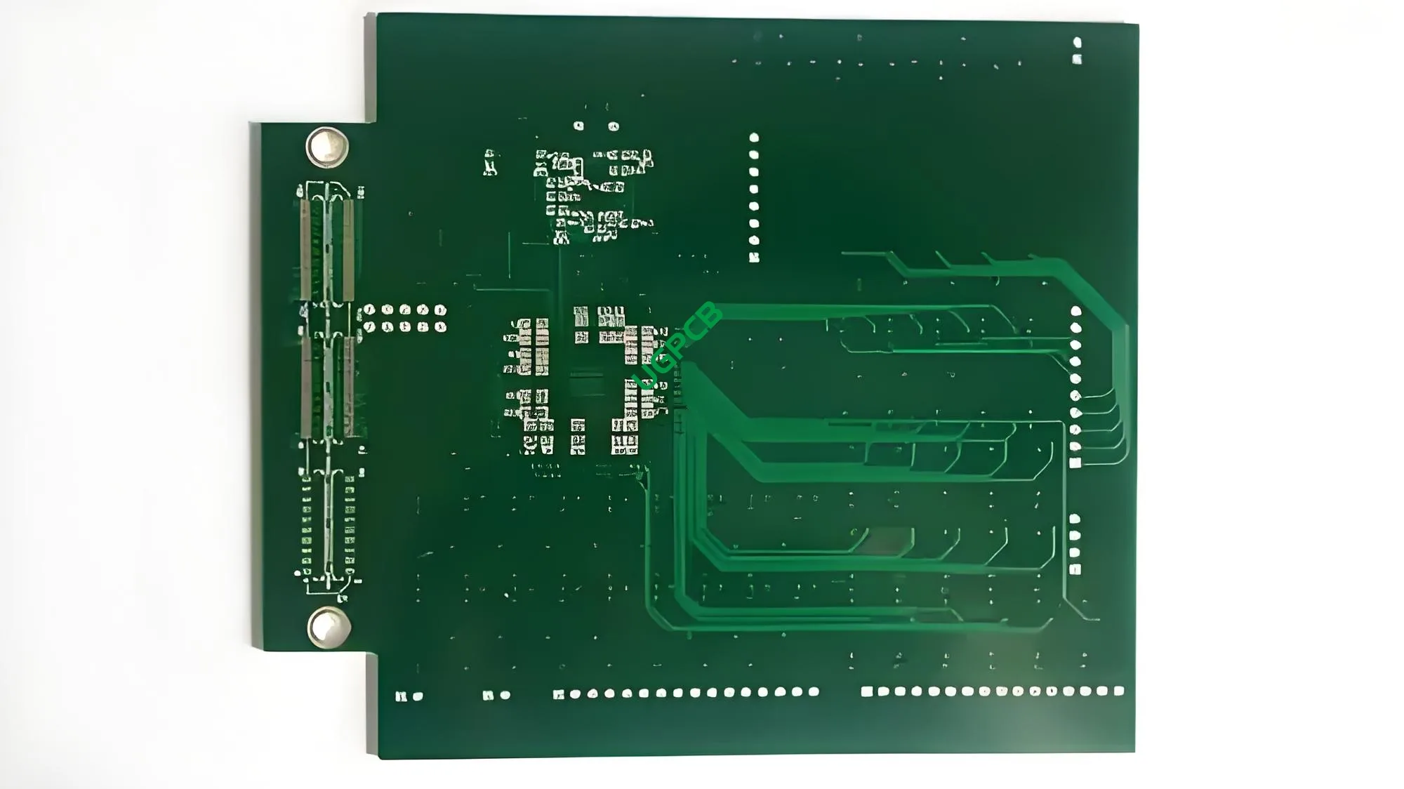
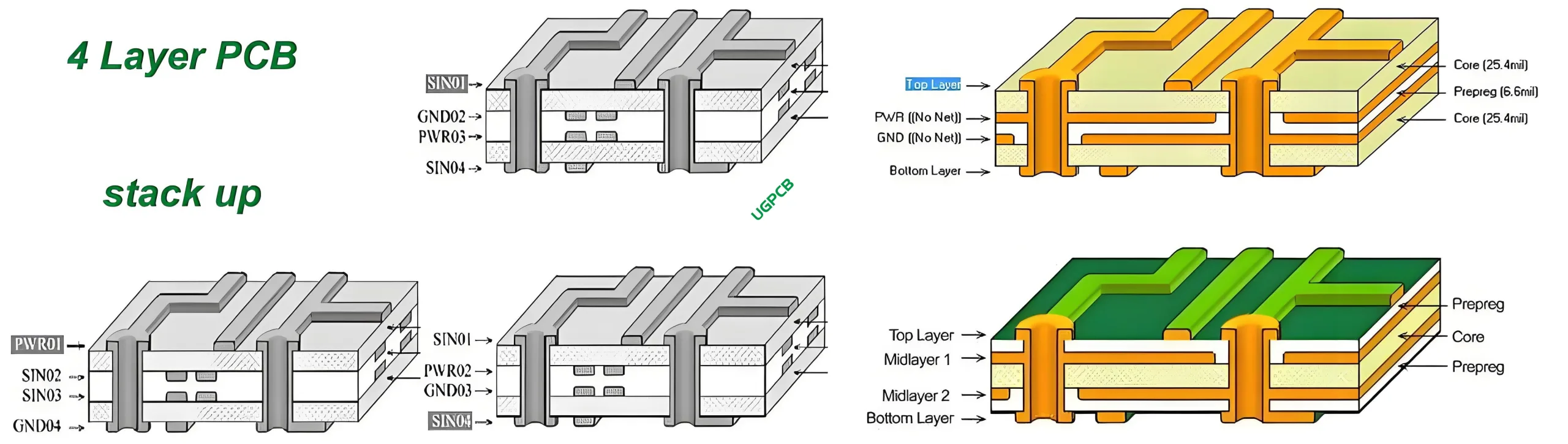
A 4-layer Printed Circuit Board (PCB) is an advanced electronic component that consists of four layers of conductive material, typically copper, separados por camadas isolantes. This multilayer structure allows for complex circuit designs with high density and improved performance.

Requisitos de design
Designing a 4-layer PCB involves several key considerations:
- Material: Commonly made from FR-4, Um material composto conhecido por suas excelentes propriedades elétricas e acessibilidade.
- Contagem de camadas: Como o nome sugere, it has four layers, which can handle more complex circuitry compared to single or double-sided boards.
- Espessura do Cobre: Can range from 0.5OZ to 6OZ, depending on the application’s power requirements.
- Tratamento de superfície: As opções incluem ouro de imersão, OSP (Conservador de solda orgânica), and lead-free HASL (Heat Activated Solder Leveling), each offering different levels of solderability and protection.
- Traço e espaço: Minimum trace and space are typically set at 3mil (0.075milímetros), permitindo detalhes finos no design do circuito.
Como funciona?
The 4-layer PCB functions by providing a platform where electronic components can be mounted and interconnected using conductive pathways etched into the copper layers. These pathways are separated by insulating layers, preventing electrical shorts while allowing signals to pass through via plated through-holes or vias.
Aplicações
Due to their complexity and reliability, 4-camada PCB are widely used in various consumer electronics including:
- Smartphones
- Comprimidos
- Laptops
- Gaming consoles
- High-end audio equipment


Classificação
4-layer PCBs can be classified based on several factors:
- Por material: Mais comumente feito de FR-4 devido ao seu equilíbrio de custo, força, e propriedades elétricas.
- By Copper Thickness: Varies from lightweight (0.5OZ) to heavyweight (6OZ) depending on the application’s needs.
- Por tratamento de superfície: As opções incluem ouro de imersão, OSP, and lead-free HASL, cada um oferecendo diferentes níveis de proteção e solda.
Materiais utilizados
The primary materials used in manufacturing 4-layer PCBs include:
- FR-4: Um laminado epóxi reforçado com vidro que fornece excelente resistência mecânica e estabilidade térmica.
- Cobre: Usado para as camadas condutas, com espessura variando com base nos requisitos de design.
- Máscara de solda: Typically green, branco, vermelho, or black, Protege os traços de cobre da oxidação e curtos -circuitos acidentais.
- Surface Treatments: Such as immersion gold, OSP, or lead-free HASL, which improve solderability and protect against corrosion.
Características de desempenho
Key performance attributes of a 4-layer PCB include:
- Alta densidade: Allows for more componentes to be packed into a smaller area.
- Confiabilidade: The use of multiple layers reduces the risk of electrical shorts and improves signal integrity.
- Integridade do sinal: Melhorou devido a caminhos de sinal mais curtos e redução de diafonia.
Composição estrutural
Estruturalmente, a 4-layer PCB comprises:
- Camadas condutivas: Feito de cobre, gravado nos padrões de circuito desejados.
- Camadas isolantes: Prevenir shorts elétricos entre camadas condutoras.
- Plated Through-Hole Vias: Facilitate connections between different layers.

Características distintas
Some notable features of a 4-layer PCB are:
- Tom fino: Permite interconexões de alta densidade, tornando -o ideal para dispositivos compactos.
- Robustez: The use of multiple layers provides a strong mechanical bond between the board and components.
- Versatilidade: Adequado para uma ampla gama de aplicações devido a contagens de camadas personalizáveis e opções de materiais.
Processo de Produção
The manufacturing process of a 4-layer PCB involves several steps:
- Design e layout: Usando software especializado para criar o padrão de circuito.
- Preparação de Materiais: Cortando materiais base para o tamanho e as superfícies de limpeza.
- Laminação: Empilhar e unir camadas individuais sob calor e pressão.
- Gravura: Removendo o excesso de cobre para formar os caminhos de circuito desejado.
- Revestimento: Adicionando uma fina camada de metal a vias e áreas de cobre expostas.
- Aplicação de máscara de solda: Applying the green, branco, vermelho, or black coating to protect traces.
- Tratamento de superfície: Applying immersion gold, OSP, or lead-free HASL for solderability.
- Inspeção Final: Garantir a qualidade e funcionalidade antes do envio.
Casos de uso
Common scenarios where a 4-layer PCB might be employed include:
- Aplicações de interconexão de alta densidade em dispositivos móveis.
- Sistemas de comunicação avançada que requerem baixa perda de sinal.
- Instrumentos médicos portáteis que precisam de desempenho confiável em ambientes severos.
- Eletrônicos automotivos exigindo robustez e longevidade.
Resumindo, the 4-layer PCB represents a significant advancement in placa de circuito impresso tecnologia, Oferecendo complexidade e desempenho incomparáveis para aplicações eletrônicas modernas. Its design flexibility combined with superior signal integrity and durability makes it an essential component in the development of next-generation consumer electronics and beyond.