

Overview of Cavity PCB
Cavitate PCB, a specialized type of printed circuit board (PCB), is designed to meet the stringent requirements of high-frequency and microwave applications. Utilizing Teflon F4MB as its core material, this product adheres to the IPC6012 Class 2 quality standard, ensuring reliable performance and durability.

Definiție și specificații cheie
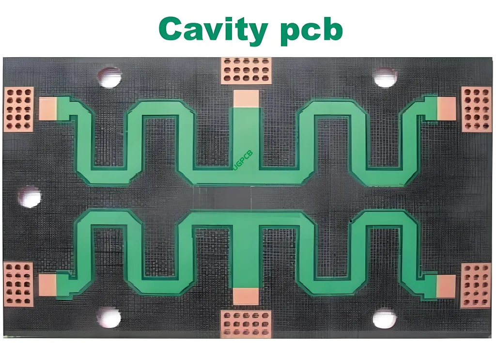
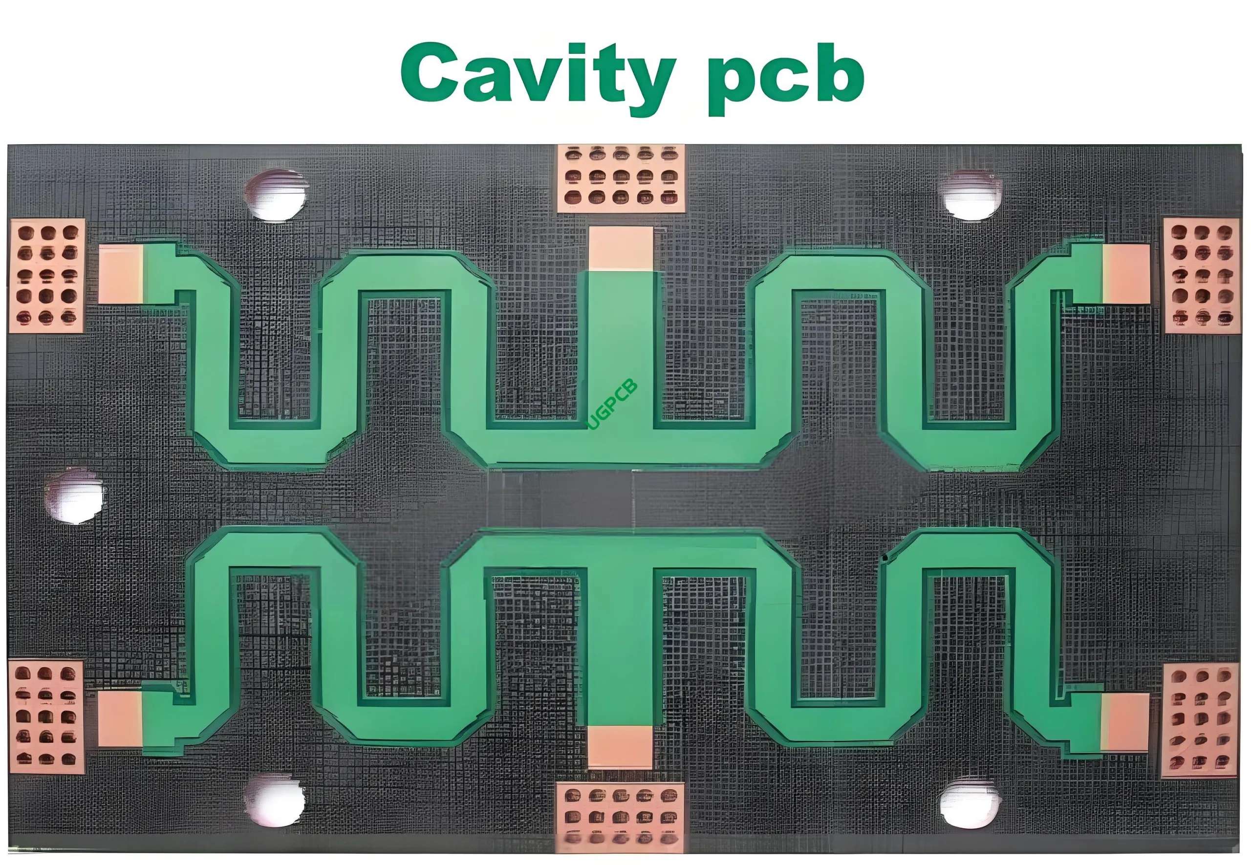
A Cavity PCB is characterized by its unique cavity structure, which is created by removing a portion of the dielectric material to form a hollowed area. This design is crucial for specific applications like power dividers, where precise control over signal distribution is necessary. The dielectric constant of Teflon F4MB is 2.55, providing stable signal transmission. The board features 2 straturi, with a total thickness of 1.5mm. The copper thickness is specified at a base of 0.5oz and a finished thickness of 1oz, ensuring efficient conductivity. The surface technology used is Immersion Silver, which offers excellent solderability and reliability.
Considerații de proiectare
When designing a Cavity PCB, several factors must be taken into account:
- Cavity Dimensions: The size and shape of the cavity should be precisely defined to match the application’s requirements.
- Dielectric Material: Teflon F4MB is chosen for its low dielectric constant and loss tangent, making it suitable for high-frequency signals.
- Grosime de cupru: Adequate copper thickness is essential for maintaining signal integrity and minimizing losses.
- Surface Finish: Immersion Silver provides a smooth and conductive surface for component attachment.
Principiul de lucru
The Cavity PCB operates based on the principle of controlled impedance and minimal signal loss. The cavity structure allows for precise control over signal routing, reducing interference and improving overall performance. The Teflon F4MB material ensures that signals maintain their integrity as they pass through the board, resulting in efficient and reliable operation.
Aplicații
Cavity PCBs are particularly suited for applications that require precise signal distribution, such as power dividers in communication systems. They are also used in radar systems, Comunicări prin satelit, and other high-frequency electronic devices where signal purity and reliability are paramount.
Clasificare
Cavity PCBs can be classified based on their layer count, cavity configuration, and specific applications. Common classifications include:
- Single-Layer and Multilayer Boards: Depending on the complexity of the circuit.
- Standard and Custom Cavities: Based on the specific requirements of the application.
- High-Frequency Specific Boards: Designed for particular high-frequency applications, often with stringent material and manufacturing standards.
Proprietăți materiale
The key properties of Teflon F4MB, the material used in Cavity PCBs, include:
- Constantă dielectrică scăzută: Asigură întârzierea și pierderea semnalului minim.
- Stable Performance Across Temperature Ranges: Maintains consistent performance in varying environmental conditions.
- High Resistance to Moisture Absorption: Prevents degradation of signal quality due to moisture ingress.
Proces de producție
The production of Cavity PCBs involves several steps:
- Selectarea materialelor: Choosing Teflon F4MB for its dielectric properties.
- Proiectarea circuitului: Creating the circuit layout with considerations for the cavity structure.
- Gravură: Eliminarea cuprului inutil pentru a crea modelul de circuit dorit.
- Cavity Formation: Precision machining to create the cavity in the dielectric material.
- Laminare: Bonding multiple layers together under high pressure and temperature.
- Finisarea suprafeței: Applying Immersion Silver for enhanced solderability.
- Testarea și controlul calității: Asigurarea că produsul final îndeplinește toate specificațiile și standardele.
Folosiți scenarii
Cavity PCBs are used in scenarios where precise signal distribution is critical, ca:
- Power Dividers: Ensuring equal distribution of signals in communication systems.
- Sisteme radar: Providing accurate and stable signal processing capabilities.
- Comunicări prin satelit: Enabling reliable data transfer between Earth and space.
În concluzie, Cavity PCBs are specialized circuit boards designed for high-frequency and microwave applications. Their unique cavity structure, combined with the properties of Teflon F4MB, makes them ideal for use in power dividers and other precision signal distribution applications.