
Искусство и наука проектирования печатных плат: Как UGPCB осваивает алхимию печатных плат
(Инженерное совершенство: от схемы до функциональной печатной платы)
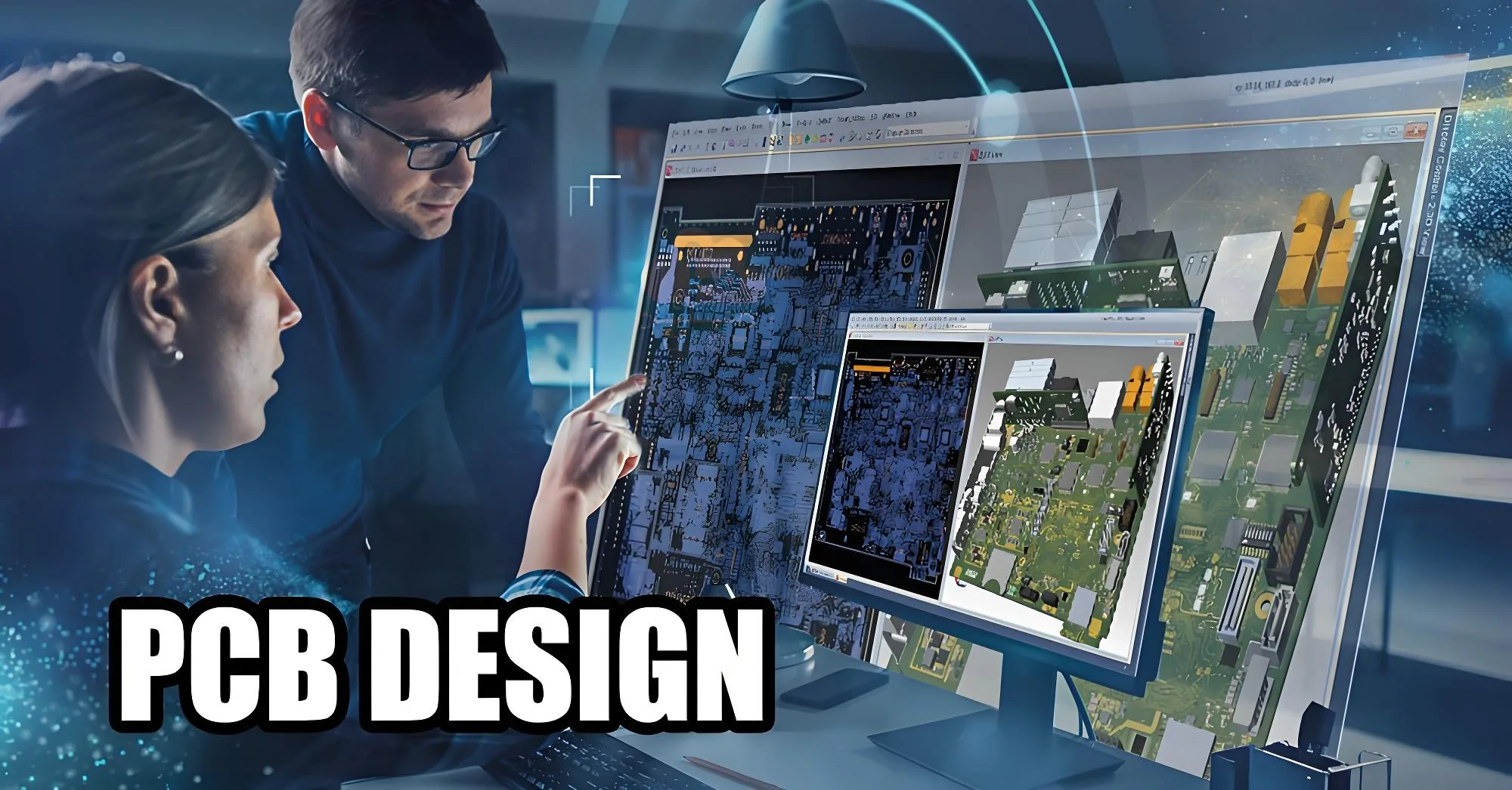

Одно неуместное переходное отверстие на 12-слойной серверной материнской плате однажды стоило технологическому гиганту $2.3 миллион отзывов. В Шэньчжэне R UGPCB&Д-центр, инженеры смотрят через тепловизионные камеры высокого разрешения, регулировка ширины дорожек с точностью до микрометра, чтобы предотвратить такие катастрофы.
С 2000+ ежегодный дизайн печатной платы проекты в аэрокосмической отрасли, медицинский, и сектора 5G, УГКПБ превращает концептуальные схемы в производственные шедевры. Их секрет? Слияние 10+ многолетний опыт и протоколы проектирования военного уровня, которые обеспечивают безотказность в критически важных приложениях.
1. Стратегический императив: Почему дизайн печатной платы определяет успех продукта
В 2024, 68% отказов электронных продуктов прослеживается до Разводка печатной платы недостатки (отчет МПК). Философия дизайна UGPCB рассматривает печатные платы как функциональные скульптуры где:
-
Каждый угол трассы 90° увеличивает электромагнитные помехи на 3-5дБ
-
0.1мм из-за несоосности может ухудшить качество сигнала 56 Гбит/с на 40%
-
Правильный тепловой расчет продлевает срок службы компонентов на 2.3Х
“PCB design isn’t drawing lines—it’s orchestrating electron highways”
— Ведущий инженер-конструктор УГКПБ
Экономический эффект ошеломляет:
-
DFM (Дизайн для производства) интеграция снижает затраты на прототипирование за счет 65%
-
Рано моделирование целостности сигнала сокращает респины на 80%
-
Стандартизированные шаблоны стека UGPCB ускоряют выход на рынок за счет 4 недели
2. Преимущество UGPCB: Инженерная ДНК расшифрована
2.1 Экосистема точного проектирования
UGPCB рабочий процесс тройной проверки устанавливает отраслевые стандарты:


Специализация по оборудованию:
-
56Гбит/с PAM4 конструкции объединительной платы
-
0.2мм шаг BGA-маршрутизация
-
20+ слой Доски HDI с 0.1ММ Микровия
-
RF-в-цифру гибридные планировки (6ГГц+)
2.2 Арсенал новейших инструментов
| Программное обеспечение | Возможности | Реализация UGPCB |
|---|---|---|
| Каденс СПБ 16.6 | 3D ЭМ моделирование, маршрутизация на основе ограничений | Проекты серверных материнских плат |
| Алтиус Дизайнер 23 | Унифицированная интеграция ECAD/MCAD | Носимые медицинские устройства |
| Сименс Экспедиция | Планирование многоплатной системы | Автомобильные блоки управления |
| Собственный тепловой ИИ | Прогнозирующее картографирование горячих точек | Мощные промышленные контроллеры |
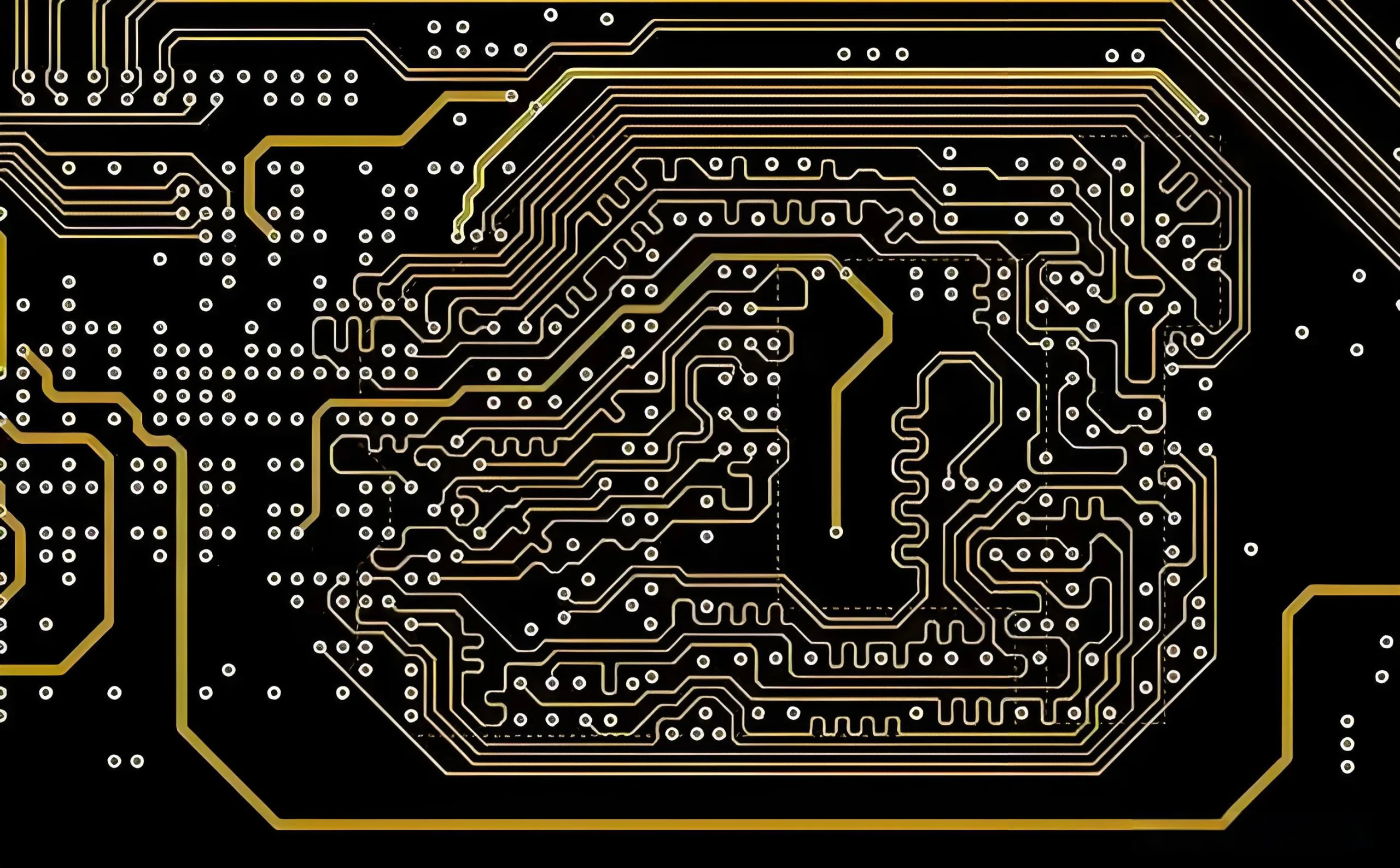
3. Алхимия трансформации цепей: Процесс проектирования UGPCB
3.1 Фаза инкубации концепции
-
Деконструкция требований: Преобразование спецификаций клиента в 23-точечные технические матрицы
-
Анализ осуществимости: Перекрестная проверка с МПК-2221 стандарты
-
План снижения рисков: Флаг 97% вопросов технологичности
3.2 Магия схематического синтеза
Инженеры УГКПБ используют:
-
База данных компонентов аналитики: 500k+ проверенных следов
-
Контроль импеданса Формулы:
![]()
(Достижимо через UGPCB 13-библиотека стека слоев)

-
Моделирование целостности электропитания:


3.3 Макет Хореография
Критические правила соблюдаются:
-
3Принцип W: Расстояние между следами = 3× ширина трассы для контроля перекрестных помех
-
10° Правило: Избегать прямоугольные изгибы в >2ГГц сигналы
-
Узоры термического рельефа: 4-Спицевые соединения для колодок QFN

4. Готовая к производству конструкция: Где искусство встречается с физикой
4.1 DFM/DFA/DFT Троица
Проверки проекта UGPCB включают в себя:
| Контрольно-пропускной пункт | Стандартный | Улучшение UGPCB |
|---|---|---|
| Щепки паяльной маски | >0.08мм зазор | Допуски 0,05 мм, определяемые лазером |
| Медный баланс | <30% асимметрия | Динамическое воровство меди |
| Кольцевые кольца | Класс МПК 3 согласие | +15% буфер допуска сверления |
| Доступ к тестовой точке | 100% чистый охват | Двусторонние измерительные сетки |
4.2 Проверка в экстремальных условиях
-
Тепловое моделирование:
Т_переход = Т_окружающая среда + (Р_θJA * P_рассеянный)
- Т_окружающая среда: Температура окружающей среды
- Единица: Градусов Цельсия (°С)
- Определение: Температура окружающей среды, в которой работает электронный компонент. Этот параметр напрямую влияет на тепловые характеристики устройства и должен измеряться в месте расположения компонента или рядом с ним..
- Р_θJA: Тепловое сопротивление перехода к окружающей среде
- Единица: Градусов Цельсия на ватт (° C/W.)
- Определение: Критический тепловой показатель, показывающий повышение температуры на ватт рассеиваемой мощности между полупроводниковым переходом и окружающей средой.. Этот параметр включает в себя все тепловые пути., включая проводимость через отведения/подушечки, конвекция, и радиация.
- P_рассеянный: Рассеиваемая мощность
- Единица: Уоттс (Вт)
- Определение: Электрическая мощность, потребляемая устройством во время работы, который преобразуется в тепловую энергию. Этот параметр имеет решающее значение для расчета повышения температуры перехода и определения требований к терморегулированию..
-
Анализ вибрации: Синусоидальные развертки MIL-STD-810G (5-2000Гц)
-
Проверка конформного покрытия: 96тесты на солевой туман в час
5. Мастерство отраслевого дизайна
5.1 Медицинская электроника
-
Безопасность пациентов:
-
8Схемы защиты от электростатического разряда кВ
-
5.5изоляционные барьеры постоянного тока кВ
-
0.001% контроль тока утечки
-
5.2 PCBA автомобильного класса
-
АЭК-Q100 сертифицированные конструкции
-
150°С управление температурой под капотом
-
КАН ФД Схема шины с сопротивлением 90 Ом ±2 %
5.3 Аэрокосмическая промышленность & Оборона
-
МИЛ-ПРФ-31032 совместимые сборки
-
Радиационно-стойкий ПЛИС
-
Резервные силовые плоскости с <5Пульсации мВ
6. Будущее спроектировано: ИИ и передовые методологии
В портфель инноваций УГКПБ входят:
-
Нейрон-Сеть ДРК: Распознавание образов для 23% Быстрее обнаружение ошибок
-
Мультифизический цифровой двойник: Параллельное тепловое, электромагнитное и механическое моделирование
-
Генеративная маршрутизация ИИ: Автономный ИЧР эвакуационная маршрутизация в 5 минуты
-
Квантовое шифрование: IP-защита через криптография на основе решетки
*”By 2026, our AI co-pilot will predict signal integrity issues before schematics are drawn”*
— Технический директор УГКПБ д-р. Лян
Почему лидеры отрасли выбирают UGPCB
-
10-Год Наследия: 10k+ успешных проектов печатных плат
-
Ноль побегов NPI: 100% гарантия технологичности
-
48-Час прототипирования: Сборка SMT с ОИ/рентген проверка
-
Безопасность военного уровня:
-
Рабочие станции с аппаратным шифрованием
-
Доступ к биометрическим данным
-
Контроль версий на основе блокчейна
-
В UGPCB, мы не просто проектируем схемы — мы проектируем надежность.
Когда спутниковая энергосистема пережила бомбардировку солнечной вспышкой в прошлом году, на его радиационно-стойкой печатной плате был нанесен наш фирменный шестиугольный узор.. От медицинских имплантатов до автономных транспортных средств, наши доски несут невидимую печать совершенства: 0.01вносимые потери дБ, 0.1°C температурная однородность, нулевая терпимость к неудачам.
[Свяжитесь с командой дизайнеров UGPCB] превратить вашу концепцию в бескомпромиссную реальность.