
При конвергенции высокоскоростных цифровых цепей и точных аналоговых систем, изысканно спроектированный печатная плата схема определяет жизнеспособность продукта - с 90% сбоев дизайна, происходящих из коллапса целостности мощности.

Когда инженеры направляют 37-й трассировку DDR4 с длиной в Altium Designer, импеданс Прерывание, спрятанные в стеках слоев, тихо разлагают целостность сигнала. Данные моделирования UGPCB показывают: ПХБ с нептимизированными модулями силовых модулей страдают 62% Показатели отказов, В то время как проекты реализации нашей технологии разделенной плоскости снижают частоту ошибок битов до 10⁻²².
Суть схем: Основные принципы схемы печатной платы & Эволюция
От диаграмм подключения до интеллектуальных систем
Современные схемы превратились в Интеллектуальные экосистемы:
-
Электрические нейронные сети: Включить 32 Правила дизайна (Ширина трассировки/расстояние/импеданс/пороги перекрестных помех); UGPCB менеджер ограничений синхронизирует 12,000+ сети
-
Междоменное сотрудничество: Анализ Allegro SI показывает ± 18 -л.с. маржиневой маржи Для критических путей в 6-слойном Доски HDI, Требование кооптимизации кооптимизации схемы-фирм-и-фирм
Революционные достижения инструмента дизайна
| Генерация инструментов | Представительное программное обеспечение | Повышение эффективности | У UGPCB случай оптимизации |
|---|---|---|---|
| Основополагающий дизайн | Протел99SE | 1X Базовая линия | Совместимость Legacy Library для миграции проекта |
| Высокоскоростной дизайн | Алтиус Дизайнер | 3.2Х | Ошибка динамического сопоставления длины ≤0,01 мм |
| Дизайн системы | Каденс Аллегро | 5.7Х | 40% Улучшение маржи схемы глаз при 16 Гбит / с |


Примерное исследование UGPCB: Миграция из Оркада в Аллегро увеличил успех маршрутизации BGA 74% к 98%, сокращение циклов развития 21 дни.
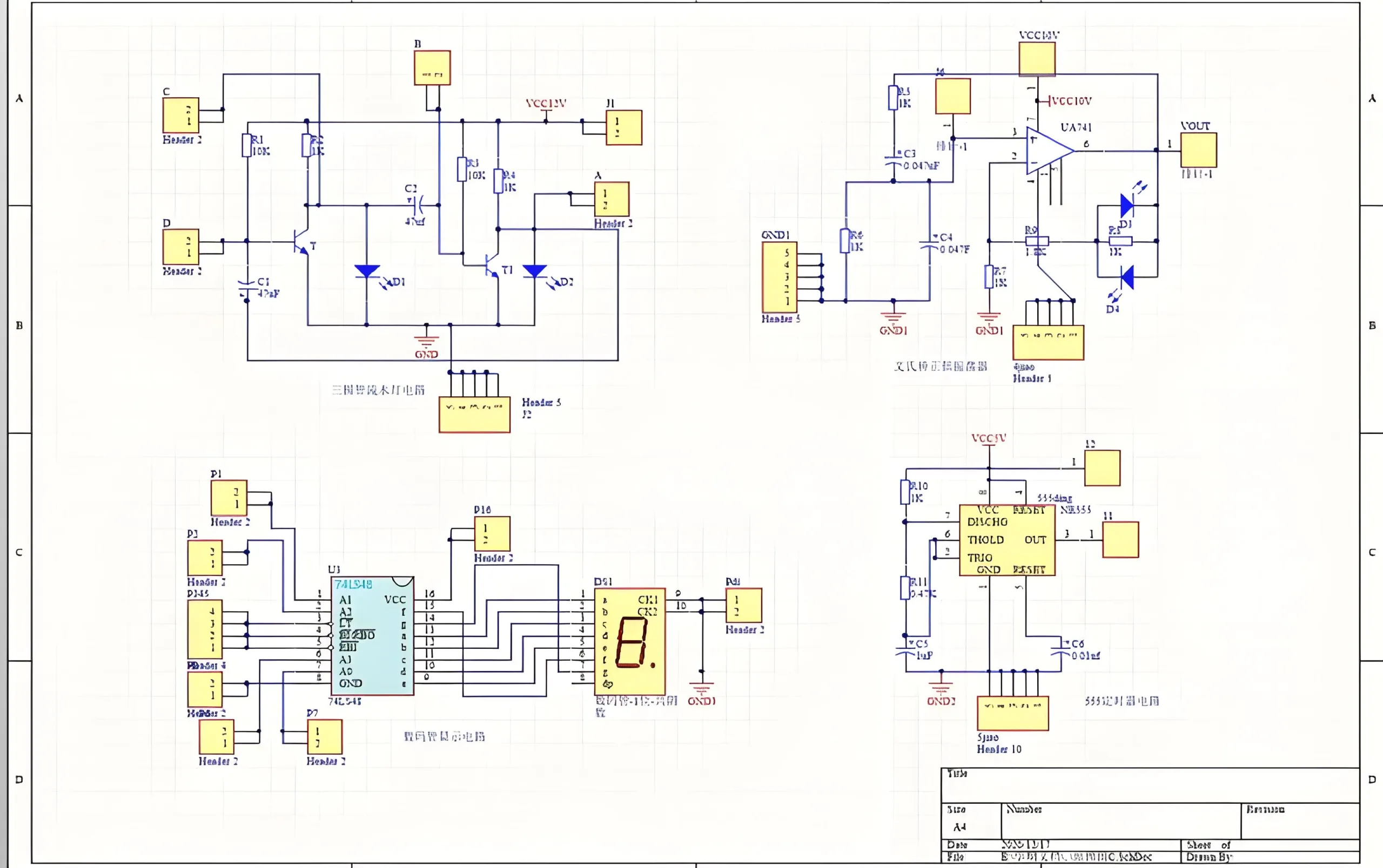
Модульная методология дизайна: Деконструирование сложных цепей
Целостность власти: Критический отличитель
Формула отбора топологии:
H = frac{P_{вне}}{P_{вне} + P_{дольдо} + P_{кондиционер}} \Quad Text{(Нацеливаться на>92\%)}
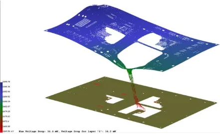
UGPCB 3D Анализ дерева мощности:
-
Снижение пониженного напряжения с 220 мВ до 35 мВ в автомобильном ECU через Оптимизация размещения LDO
-
Гибридные плоскости: Методы разделения/смешанной плоскости уменьшились 67%

Точный контроль высокоскоростных сигнальных путей
Уравнение контроля импеданса:
Реализация UGPCB:
-
Дифференциальная пара компенсаций: Достиг перекоса<2PS в оптических модулях 100G
-
Эм защитные стены: 18DB SNR улучшение в медицинский печатная плата через цифровую/аналоговую изоляцию
Промышленный дизайн: UGPCB 9 Основные технологии
3D Оптимизация архитектуры Stackup
Оптимальная 8-слойная конфигурация:
L1: Сигнал (Высокоскоростной)
L2: Solid GND
L3: Сигнал (Стрип -линия)
L4: Power
L5: GND
L6: Signal
L7: Power
L8: Сигнал (Низкая скорость)
Валидация: 12DBμV/M EMI восстановление, FCC Class B Сертифицирован
Производственный дизайн (DFM) Точность
UGPCB ± 0,025 мм управление процессом:
-
Технология микровий: 0.1ММ лазерные тренировки, 12:1 Соотношение сторон
-
Толщина меди: ± 10% толерантность к травлениям для наружных слоев 2 унций
-
Припаяя маска мостов: 0.075Минимальная ширина мм предотвращает мостику SMT
За пределами дизайна: Полный жизненный цикл UGPCB
Обеспечение целостности сигнала
Фаза дизайна: Hyperlynx Pre-Layout 90% риски
Фаза проверки: Тестирование TDR обеспечивает <5% импедансное отклонение
Массовое производство: Золотая справочная база данных для управления параметрами ключа
Интеллектуальная интеграция производства


Результаты: 48-Часовой прототип доставки, 99.2% Выход первого прохода
Будущая лаборатория: Технологические границы UGPCB
Силиконовая субстратная гетерогенная интеграция
2.5D TSV Interposers:
-
0.3ММ межсоединения для интеграции FPGA-HBM
-
Термическая сопротивление уменьшено до 0,15 ° С/Вт.
Руководящая Эда революция
NeuroRoute Engine:
-
8X Повышение эффективности маршрутизации
-
Функция оптимизации:
Min(ΔL, Crosstalk, Via_Count) -
Развернуто в массиве антенн 5G MMWave печатная плата дизайн