
В области электронной техники, количество слоев Печатная плата (печатная плата) часто является прямым показателем сложности и технологичности продукта.. Хотя большинство инженеров обычно работают с 2, 4, or 6-layer boards—with consumer electronics even employing cost-optimized solutions like “pseudo-8-layer” boards (6 функциональные электрические слои плюс 2 изоляционные слои по толщине)— ситуация резко меняется в сфере высокопроизводительных серверов, высокопроизводительные компьютерные материнские платы, и новейшее коммуникационное оборудование. Здесь, печатные платы с 16, 32, или даже 64 слои общие. Это поднимает критический вопрос: каковы основополагающие принципы проектирования и технологии производства, которые позволяют это сделать? печатные платы с большим количеством слоев? В этой статье представлен углубленный анализ технических аспектов., основные проблемы, и передовые производственные решения для печатных плат с большим количеством слоев.
Почему печатные платы с большим количеством слоев? Больше, чем просто игра по маршрутизации
Увеличение количества слоев печатной платы — это не погоня за впечатляющими цифрами.. Фундаментальным драйвером является экспоненциальный рост требований к производительности современных электронных устройств.. Когда плотность выводов чипа продолжает расти (например, BGA-корпусы с более чем 2500 шарики припоя), скорости сигнала переходят в режим ГГц (например, PCIE 5.0 в 32 ГТ/с), и системы должны одновременно обрабатывать высокоскоростные цифровые, РЧ аналог, и мощные сигналы, традиционный 4 или 6-слойные платы становятся неадекватными.
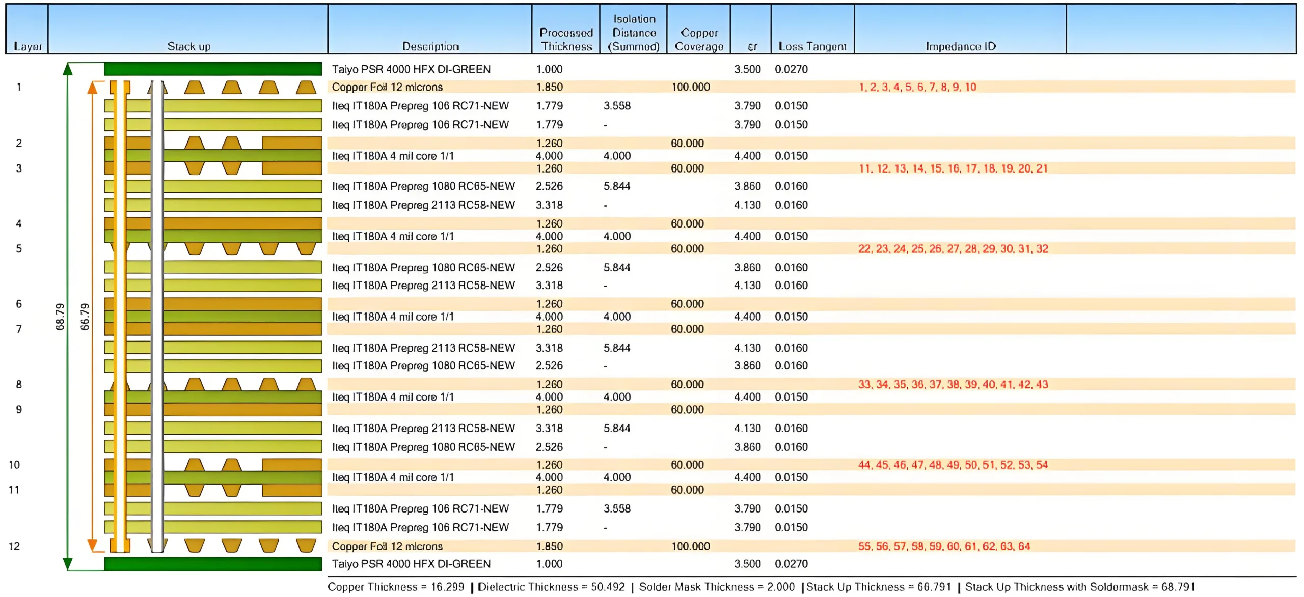
Основная ценность печатных плат с большим количеством слоев заключается в обеспечении достаточных ресурсов маршрутизации и полных опорных плоскостей.. Типичная сборка 12-слойной платы может выглядеть так:: Сигнал 1 / Земля / Сигнал 2 / Власть 1 / Сигнал 3 / Земля / Сигнал 4 / Власть 2 / Сигнал 5 / Земля / Сигнал 6. This symmetrical “ground-signal-power-signal-ground” stack-up (следуя рекомендациям, таким как IPC-2141A) эффективно контролирует импеданс и обеспечивает малошумящий обратный путь для высокоскоростных сигналов. Статистика показывает, что в таком оборудовании, как коммутаторы центров обработки данных, конструкции с использованием печатных плат с 20+ уровни могут уменьшить перекрестные помехи в критических сетевых сигналах более чем 60% (данные взяты из отчета IPC TR-579.).

Проблемы проектирования печатных плат с большим количеством слоев: Beyond “Drawing Traces”
Целостность сигнала и контроль импеданса
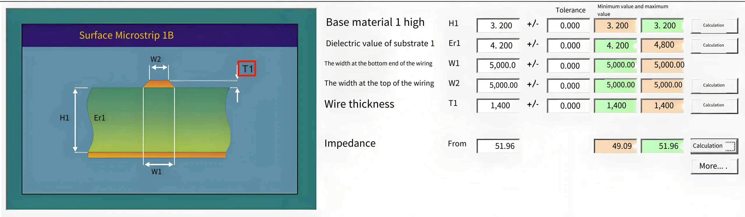
В высокоскоростном исполнении, Трассы печатной платы больше не являются простыми электрическими соединениями, а должны представлять собой точно контролируемые линии передачи.. Отклонения волнового сопротивления (например, 50Ом несимметричный, 90Дифференциал Ом/100 Ом) непосредственно вызывать отражение сигнала, промахнуться, и закрытие глазковой диаграммы данных. Импеданс в первую очередь зависит от ширины дорожки. (Вт), Диэлектрическая толщина (ЧАС), диэлектрическая проницаемость (εr), и толщина меди. Стандартные инструменты, такие как Polar Si9000, моделируют это с использованием упрощенных формул. (Для микрополосков):
Z0 ≈ (87 / √(εr + 1.41)) * ln(5.98 * H / (0.8 * W + T))
где T — толщина следа. Для обычного материала FR-4 (εr ≈ 4.2 @ 1 ГГц), для достижения импеданса 50 Ом при толщине диэлектрика H=5 мил, ширину дорожки W необходимо контролировать примерно на уровне 8.5 мил. Однако, неоднородность ламинированной структуры многослойных плит, эффект стеклянного переплетения, и производственные допуски на травление (обычно ±10%) все они приводят к изменениям импеданса. Стандарт IPC-6012D допускает отклонение измеренного значения ±10 % от номинального импеданса для плат с контролируемым импедансом., но высокопроизводительные приложения теперь требуют допусков до ±7%..

Целостность электропитания и управление температурным режимом печатной платы
По мере увеличения количества слоев, сложность распределительной сети (ПДН) дизайн растет в геометрической прогрессии. Напряжение ядра может составлять всего 0,8 В, а переходные токи достигают сотен ампер.. В этом сценарии, целевой импеданс силовых плоскостей должен быть чрезвычайно низким (например, <1 МОм) для подавления пульсаций напряжения. Это требует тщательного планирования размещения развязывающего конденсатора., оптимизация межплоскостной емкости между силовыми и земляными плоскостями (рассчитывается по C = ε0 * εr * A / d, где A — площадь перекрытия, а d — толщина диэлектрика.), и может потребоваться выделение выделенных уровней питания. Более того, повышенная плотность мощности за счет высокой плотности маршрутизации (превышающий 100 Вт/см² в некоторых областях ASIC) требует усиленного охлаждения за счет тепловых массивов, встроенные медные монеты, или металлические подложки, еще больше усложняет проектирование и обработку стека.
Алхимия производства печатных плат: Прецизионная технологическая цепочка для многослойных плат
Преобразование дизайна в физическую реальность представляет собой еще одну серьезную проблему для печатных плат с большим количеством слоев.. The core process can be summarized as a precise cycle of “lamination – alignment – drilling – plating.”
Выравнивание слоев: Искусство регистрации на микронном уровне
Все слои многослойной платы (внутренние слои и препрег) должны быть ламинированы в единое целое под воздействием высокой температуры и давления.. Несовпадение слоев может привести к тому, что сверла срежут следы., создать шорты, или вызвать разрывы импеданса. Для 16-слойной платы, если средняя ошибка выравнивания на слой равна 25 мкм (допуск графической регистрации, разрешенный классом IPC-A-600G 3), в худшем случае совокупная ошибка может превысить 100 мкм — достаточно, чтобы скомпрометировать 0.2 контактная площадка BGA мм.
Ведущие производители, такие как UGPCB, решают эту задачу, используя Лазерная прямая визуализация (LDI) и высокоточные системы оптического выравнивания. Выравнивающие штифты и глобальные реперные шкалы выгравирован на каждом основном слое, в сочетании с захватом изображения CCD и серворегулировкой, может контролировать послойную регистрацию внутри 15 мкм (данные основаны на технических описаниях процессов ведущих поставщиков отрасли.). Кроме того, анализ реологии материала прогнозировать растекание смолы и ориентацию стекловолокна препрега во время ламинирования, позволяет предварительно компенсировать размерную деформацию, обеспечение равномерной толщины диэлектрика после прессования.
https://example.com/pcb-lamination-alignment.png
Изображение Alt Text: Подробное объяснение процесса ламинирования и выравнивания многослойной печатной платы., показ лазерных целей, оптическое выравнивание, и поток ламинирования, обеспечение высокой точности послойной регистрации.
Через соединение: От «сквозных отверстий» к ИЧР любого уровня
Традиционные сквозные отверстия пронизывают всю толщину плиты., занимают значительное пространство маршрутизации на печатных платах с большим количеством слоев и вызывают проблемы с длинным трактом возврата сигнала. Поэтому, Взаимодействие высокой плотности (ИЧР) технология обеспечивает более гибкие переходы между слоями, используя слепые переходы (от поверхности к внутреннему слою), скрытые переходные отверстия (внутренний слой к внутреннему слою), и Микровия (диаметр ≤ 0.15 мм).
Например, a “1+N+1” HDI structure (где поверхностные слои используют микроотверстия, а средний представляет собой традиционное ядро из N-слоя) может увеличить плотность маршрутизации более чем 40% без увеличения общего количества слоев (ссылка на стандарт проектирования IPC-2226 HDI). Однако, это вносит такие сложности в процесс, как последовательное сверление ламината, посредством наполнения и покрытия, и несколько циклов ламинирования. Производители должны оборудовать лазерные сверлильные станки (для микроотверстий), вертикальные вакуумные укупорочные машины (для обеспечения заполнения без пустот), и оборудование плазменной очистки (удалить следы сверления), и строго выполнять Тестирование летающих зондов и четырехпроводное тестирование по Кельвину проверить надежность каждой точки соединения.
Будущие тенденции: Инновации в материалах и интеграция проектирования и производства на основе моделирования
Эволюция печатных плат с большим количеством слоев продолжается. По мере увеличения скорости сигнала до 56 Гбит/с и выше с использованием модуляции PAM4, материалы с низкими потерями (как Панасоник МЕГТРОН 6, Rogers RO4000 Series) с εr всего лишь 3.2 и факторы рассеяния (Дф) ниже 0.002 принимаются. Одновременно, встроенные компоненты (как скрытые резисторы и конденсаторы) и интеграция полупроводниковых пакетов (например, EMIB компании Intel, SoIC TSMC) стирают границы между печатными платами и микросхемами.
Для проектировщиков и специалистов по закупкам, выбор квалифицированного количество верхних слоев поставщик печатных плат имеет первостепенное значение. Помимо сосредоточения внимания на своих максимальная возможность слоя (например, стабильное массовое производство 32 слои), контроль импеданса способность (предоставляют ли они отчеты об испытаниях импеданса), и Уровень процесса ИЧР (минимальный размер отверстия/ширина дорожки), крайне важно оценить их услуги по поддержке дизайна (например, моделирование SI/PI и советы по оптимизации стека) и система контроля качества (соответствие классу МПК 3 стандарты и наличие комплексного инспекционного оборудования, такого как AOI, АВИ, 3D рентген).

В поисках высокой надежности, высокопроизводительный многослойная печатная плата решение? Обращение к профессиональному поставщику с возможностями полной цепочки от моделирования проектирования до точного производства, чтобы получить индивидуальное проектное предложение по штабелированию и мгновенная цитата для вашего проекта – это первый важный шаг на пути к успеху. В эпоху Интернета всего и вычислительного взрыва, Печатные платы с большим количеством слоев больше не являются просто носителями; они являются краеугольным камнем, определяющим пределы производительности электронных систем..