

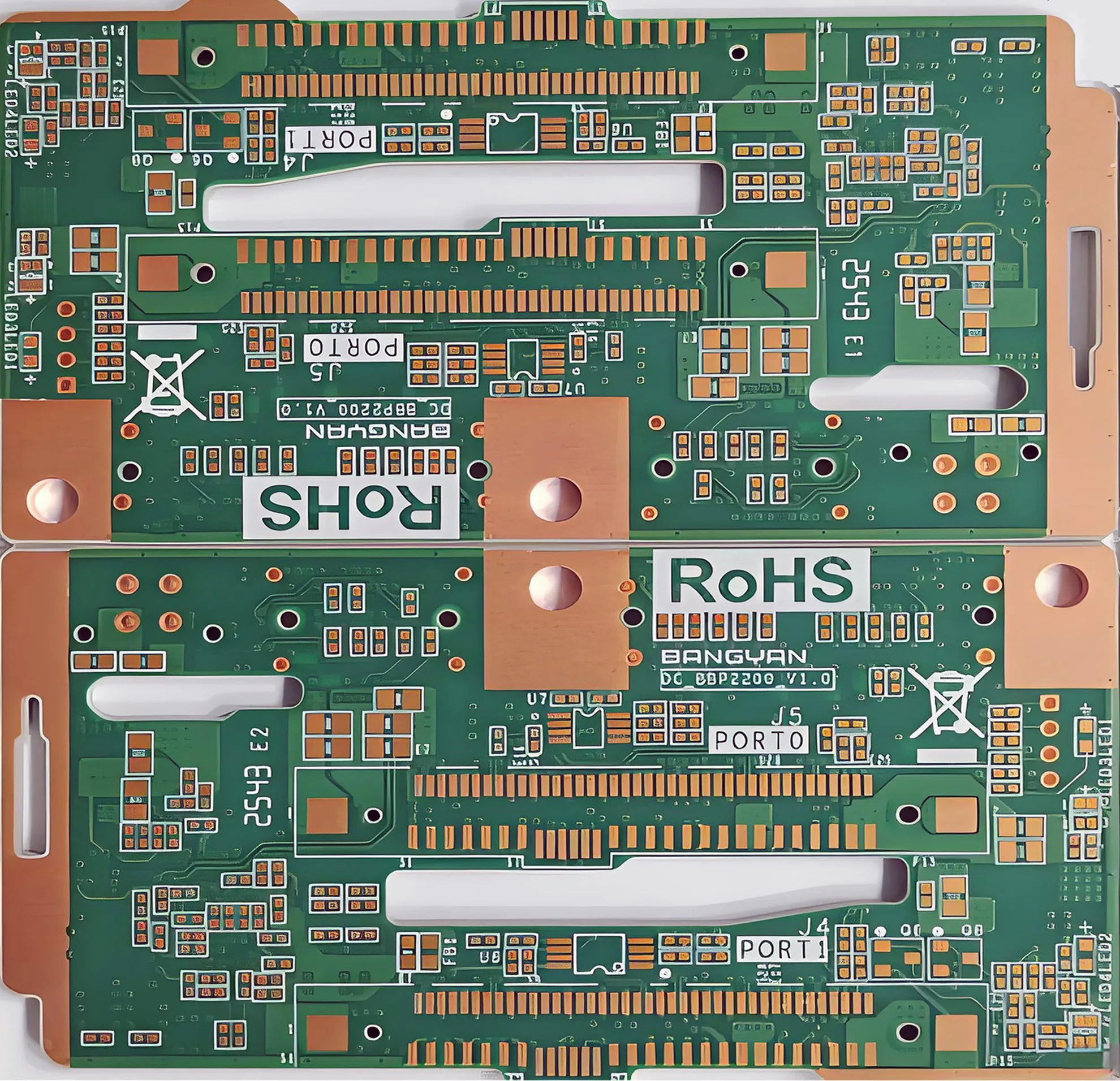
Обзор профессионального продукта: 12-слойная высокоскоростная, Печатная плата высокой плотности
В эпоху высокоскоростной передачи данных и сложной системной интеграции, обычные печатные платы (печатные платы) не соответствуют требованиям к производительности современной электроники. The 12-слой высокоскоростной, Высокая печатная плата это инженерное решение. До 12 точно выровненные проводящие слои, он обеспечивает сложные соединения и эффективную передачу сигналов при компактных размерах., выступая в качестве “центральная нервная система” для высокопроизводительного сетевого оборудования, серверы дата-центра, высокопроизводительные вычисления (HPC), и оборудование искусственного интеллекта.
Как эксперт Производитель печатных плат и поставщик печатных плат, UGPCB использует передовые процессы для обеспечения надежного 12-слой печатная плата производство, обеспечение конкурентоспособности вашей продукции.
Углубленный анализ параметров: Основа производительности
Возможность высококачественного многослойная печатная плата определяется его спецификациями. Ниже приведен анализ основных параметров этого продукта.:
-
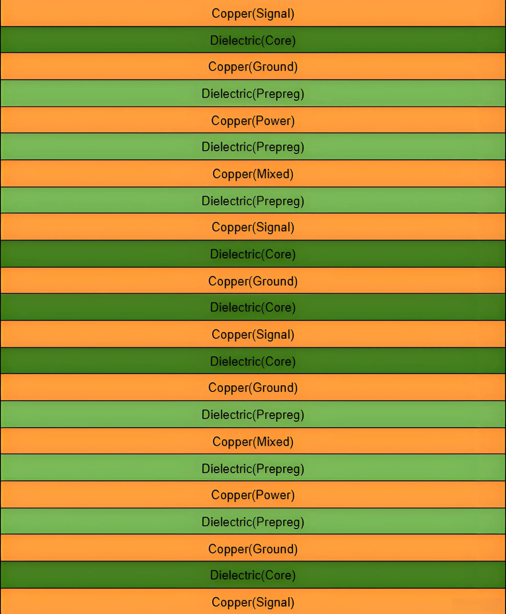
Количество слоев & Стек-ап: 12 слои. Этот многослойный дизайн печатной платы обеспечивает превосходную целостность сигнала (И), целостность власти (ПИ), и производительность EMC по сравнению с платами с меньшим количеством слоев. Это позволяет использовать выделенные силовые и заземляющие плоскости., обеспечение четких путей возврата для высокоскоростных сигналов.
-
Толщина доски & Толерантность: 2.4мм ±10%. Такая прочная толщина обеспечивает превосходную механическую прочность для объединительных плат и приложений большого форм-фактора., обеспечение надежности при стыковке и монтаже. Жесткие допуски гарантируют последовательность сборки..
-
Вес готовой меди: Уникальное распространение:
1/1/1/1/1/2/2/1/1/1/1/1 oz. Это указывает на то, что внутренние слои (16 -й & Л7) используйте 2 унции тяжелой меди, разработан специально для подачи сильноточной мощности. Внешний и другие сигнальные слои используют медь толщиной 1 унцию., оптимизирован для травления тонких линий. Эта гибридная конструкция является визитной карточкой высокая надежность Изготовление печатной платы. -
Возможности критического процесса:
-
Минимальный размер просверленного отверстия: 0.2мм. Поддерживает разветвление BGA высокой плотности., повышение гибкости маршрутизации.
-
Минимальная ширина линии/пространство: 0.076мм / 0.09мм (3мил / 3.5мил). Достигает Взаимодействие высокой плотности (ИЧР)-уровень маршрутизации, необходим для высокоскоростного распространения сигнала.
-
-
Поверхностная отделка: ОСП (Органическая припаяя консервант). Совместим как со свинцовой, так и с бессвинцовой пайкой., защищает медные площадки от окисления, обеспечивает превосходную плоскостность поверхности, и экономически эффективен — идеально подходит для плат с плотным поверхностным монтажом. компоненты.
Основные материалы & Ключевые технологии: Обеспечение превосходной целостности сигнала
-
Высококачественный ламинат: Использует Наня NY6300S высокоскоростной ламинат. Высокая температура стеклования. (Тг >150°С) обеспечивает стабильность размеров и надежность при высокотемпературной пайке оплавлением. Оптимизированная диэлектрическая проницаемость (Дк) и коэффициент рассеивания (Дф) значительно снизить потери сигнала на высоких частотах, образуя материальную основу для высокочастотные печатные платы.
-
Усовершенствованная медная фольга: Нанимает РТФ (Фольга с обратной обработкой) медь. По сравнению со стандартным электроосажденным (Редакция) фольга, Фольга RTF имеет более гладкую поверхность., низкопрофильная поверхность на обработанной стороне. Это уменьшает потери сигнала из-за “скин-эффект” на высоких частотах, критически улучшая характеристики дифференциальных сигналов, превышающих 10 Гбит / с.
-
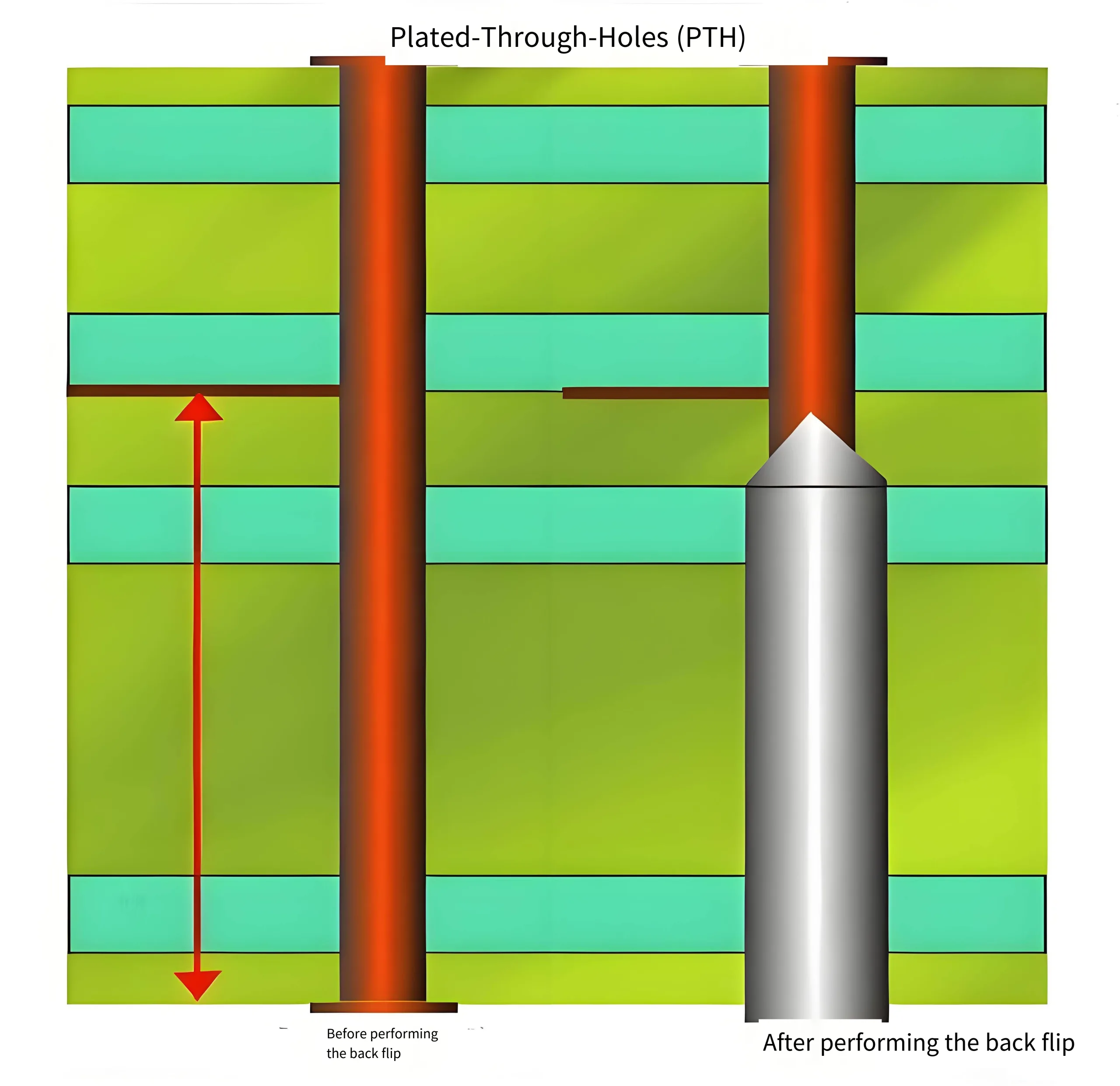
Критический процесс: Бурение с контролируемой глубиной (Назад бурение): В 12 слоев или выше Многослойные печатные платы, неиспользованная часть (заглушка) сквозного отверстия может вызвать значительное отражение сигнала, унижающее целостность. The процесс обратного сверления точно убирает этот нефункционал через заглушку, устранение его негативного воздействия — ключевая технология высокоскоростная многослойная печатная плата производительность.
Производственный поток & Гарантия качества
UGPCB 12-Процесс производства печатной платы. строго придерживается Стандарты IPC и включает в себя Дизайн для производства (DFM) обзор, визуализация внутреннего слоя, ламинирование, бурение (включая обратное сверление), покрытие, визуализация внешнего слоя, нанесение паяльной маски, обработка поверхности (ОСП), маршрутизация, электрические испытания, и окончательная проверка. Каждый этап поддерживается прецизионным измерительным оборудованием. (АОИ, Тестирование импеданса, Тест летающего зонда), обеспечение каждого монтажная плата Поставленный продукт соответствует проектным спецификациям и нашим высоким стандартам качества..
Типичные приложения & Классификация продуктов
Этот высокопроизводительный печатная плата предназначен для требовательных электрических сред и сложных систем, в основном используется в:
-
Высококачественная сеть & Коммуникационное оборудование: Материнские платы Core для оптических модулей 400G/800G, высококлассные маршрутизаторы, и переключатели.
-
Дата-центр & Облачные вычисления: Серверные материнские платы, карты-ускорители, объединительные платы хранения данных.
-
Высокопроизводительные вычисления: Материнские платы для рабочих станций, Вычислительные карты с графическим процессором, Аппаратное обеспечение ускорителя искусственного интеллекта.
-
Расширенный тест & Измерительные приборы: Внутренние платы для приборов, обрабатывающих очень высокочастотные сигналы.
Классификация научной продукции:
-
По количеству слоев: Многослойная печатная плата (>8 слои)
-
По типу технологии: Высокоскоростная/высокочастотная печатная плата, HDI печатная плата, Тяжелая медная печатная плата (частичный)
-
По приложению: Плата телекоммуникационной инфраструктуры, Плата центра обработки данных/сервера
Почему стоит выбрать UGPCB для вашей 12-слойной высокоскоростной печатной платы?
-
Техническая экспертиза: Доказанное мастерство обратное бурение и Медная фольга RTF приложение для решения задач высокоскоростного проектирования.
-
Точное производство: Способен 3/3.5 мил линия/пробел, соответствие строгим требованиям к межсоединениям высокой плотности.
-
Целостность материала: Основное использование авторитетных высокоскоростные ламинаты как Nanya NY6300S, обеспечивает базовую производительность.
-
Поддержка дизайна: Эксперт дизайн печатной платы и Обзор ДФМ услуги для снижения рисков вашего проекта с самого начала.
-
Постоянное качество: Полностью контролируемый Производство печатных плат и система контроля поставляют надежную продукцию, которой можно доверять.
Готовы улучшить ваше оборудование? Свяжитесь с инженерами УГКПБ для получения бесплатное предложение печатной платы и DFM -анализ в вашем следующем проекте высокоскоростной 12-слойной платы.


Этот веб-сайт может быть обзором данных, которые вы хотели по этому поводу и не знали, кому следует. Взгляните сюда, и ты полностью обнаружишь это.