


Communications PCBs Applications
Communications PCBs are also used in general telecommunications systems such as cell towers, спутники, high-speed routers and servers, and commercial telephony. Telecom PCBs are also frequently used to control LED displays and indicators.
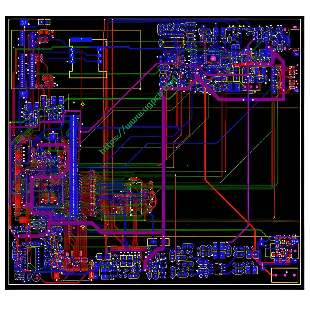
Structure and Composition of High-Frequency Hybrid Splint
Base Plate and Wire Layers
Высокочастотная гибридная шина включает в себя опорную пластину., который сложен и расположен на первом внутреннем слое проволоки, первый внешний слой проволоки, и верхняя поверхность слоя чернил паяльной маски сверху вниз по порядку снизу вверх.
Solder Resist Ink Layer and Substrate Areas
The second layer of solder resist ink layer, the substrate includes a high-frequency area and an auxiliary area. Вспомогательная зона наконец-то исправлена, а вкладка в области ВЧ должна располагаться в фиксированном положении.
Functionality and Material Usage
Utility Model Description
В полезной модели предусмотрена высокочастотная гибридная шина., который разделен на две части: высокочастотная зона и вспомогательная зона. It provides mechanical support.
High-Frequency Area Arrangement
В полезной модели указано, что высокочастотная область организована самостоятельно., and only the high-frequency area is made of high-frequency materials. Under the condition of satisfying high-frequency signals, the use of high-frequency board materials is minimized and the production cost is reduced.