
Введение в 4 Layers Industrial Control PCBA
Обзор
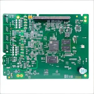
The 4 Layers Industrial Control PCBA is a sophisticated сборка печатной платы designed for industrial control applications. It features four layers of conductive material, which allows for complex circuitry and high-density компонент размещение. This PCBA is essential for various industrial automation and control systems due to its reliability and performance.

Определение
А 4 Layers Industrial Control PCBA refers to a multi-layer printed circuit board assembly that incorporates four layers of copper traces, separated by dielectric layers. This design enables more compact and efficient circuit designs suitable for industrial environments.
Принцип работы
The working principle of a 4 Layers Industrial Control PCBA involves the use of multiple layers of conductive copper traces embedded within non-conductive substrate layers. These layers are interconnected through vias (plated-through holes) to allow electrical signals to travel between different layers. The surface mount technology (СМТ) and through-hole technology (ТТТ) components are soldered onto the печатная плата, creating a functional circuit.
Приложения
Этот тип печатная плата is widely used in industrial control systems, включая:
- Automation equipment
- Robotics
- Machine control units
- Sensor interfaces
- Power distribution boards

Классификация
PCBA можно классифицировать по нескольким критериям.:
- По количеству слоев: Односторонний, двусторонний, многослойный (включая 4 слои)
- По типу компонентов: Сквозное отверстие, поверхностный монтаж, или комбинация того и другого
- By industry standards: RoHS compliant, бессвинцовый, и т. д..
Материалы
The primary materials used in the construction of a 4 Layers Industrial Control PCBA include:
- Copper foil for the conductive layers
- Fiberglass or composite materials for the dielectric layers
- Без свинца Hasl (Heat Sink Assembly Level) обработка поверхности
- Green solder mask for protection and insulation
Производительность
Производительность этой печатной платы характеризуется:
- Высокая теплопроводность благодаря медным слоям
- Низкие потери сигнала и высокая целостность сигнала
- Resistance to environmental factors such as humidity, temperature variations, and mechanical stress
- Соответствие RoHS и стандартам сборки, не содержащими свинца.
Структура
The structure of a 4 Layers Industrial Control PCBA typically includes:
- Four layers of copper traces separated by dielectric layers
- Варенья (plated-through holes) for inter-layer connectivity
- Surface mount and through-hole components soldered onto the board
- A green solder mask covering the top layer for protection and identification
Функции
Ключевые особенности этой печатной платы включают в себя:
- High density and compact design suitable for space-constrained applications
- Превосходные возможности управления температурным режимом
- Enhanced durability and longevity in harsh industrial environments
- Compatibility with a wide range of electronic components
Производственный процесс
The production process of a 4 Layers Industrial Control PCBA involves several steps:
- Дизайн: Использование специализированного программного обеспечения для создания схемы схемы и размещения компонентов..
- Подготовка материала: Selecting and preparing the copper foil, dielectric layers, и другие материалы.
- Наложение слоев: Укладка слоев меди и диэлектрических материалов.
- Через сверление: Сверление отверстий в сложенных слоях для переходных отверстий..
- Покрытие: Покрытие переходных отверстий медью для обеспечения электрического соединения..
- Офорт: Удаление лишней меди для формирования желаемого рисунка схемы..
- Размещение компонентов: Soldering surface mount and through-hole components onto the PCB.
- Тестирование: Проведение тщательного тестирования для обеспечения функциональности и соответствия стандартам..
- Заключительная проверка: Обеспечение соответствия печатной платы всем критериям качества и производительности..


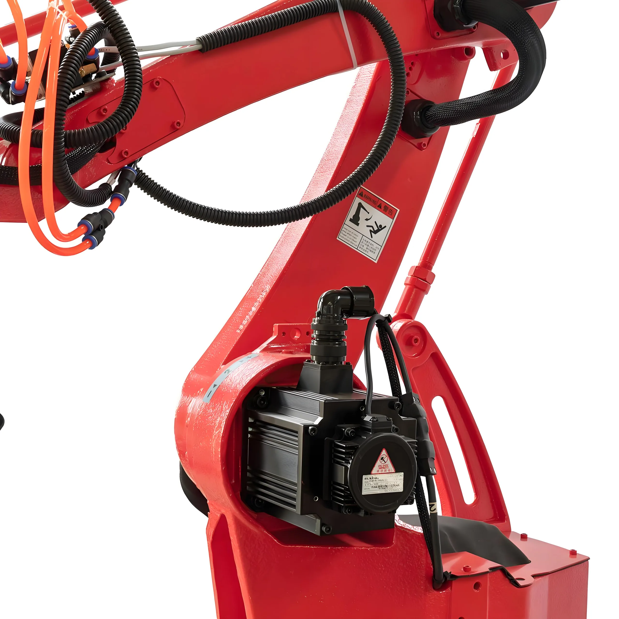
Варианты использования
Common use cases for the 4 Layers Industrial Control PCBA include:
- Industrial automation systems where high reliability and performance are crucial
- Robotic arms and machinery requiring precise control
- Manufacturing plants with demanding environmental conditions
- Power distribution and control panels in heavy industries
Заключение
The 4 Layers Industrial Control PCBA is an advanced and reliable solution for various industrial control applications. Its multi-layer design, высокопроизводительные материалы, and compliance with industry standards make it an ideal choice for engineers and manufacturers seeking robust and efficient electronic solutions.