
In the field of electronic engineering, the layer count of a แผงวงจรพิมพ์ (พีซีบี) is often a direct indicator of a product’s complexity and technological sophistication. While most engineers routinely work with 2, 4, or 6-layer boards—with consumer electronics even employing cost-optimized solutions like “pseudo-8-layer” boards (6 functional electrical layers plus 2 insulation layers for thickness)—the landscape shifts dramatically in high-end servers, high-performance computing motherboards, and cutting-edge communication equipment. ที่นี่, PCBs with 16, 32, or even 64 layers are common. This raises a critical question: what are the underlying design principles and manufacturing technologies that enable these high-layer count PCBs? This article provides an in-depth analysis of the technical aspects, core challenges, and advanced manufacturing solutions for high-layer count PCBs.
Why High-Layer Count PCBs? More Than Just a Routing Game
Increasing PCB layer count is not about pursuing impressive numbers. The fundamental driver is the exponential growth in performance demands of modern electronic devices. When chip pin density continues to rise (เช่น, BGA packages with over 2500 solder balls), signal speeds enter the GHz regime (เช่น, PCIE 5.0 ที่ 32 GT/วินาที), and systems must simultaneously handle high-speed digital, RF analog, and high-power signals, traditional 4 or 6-layer boards become inadequate.
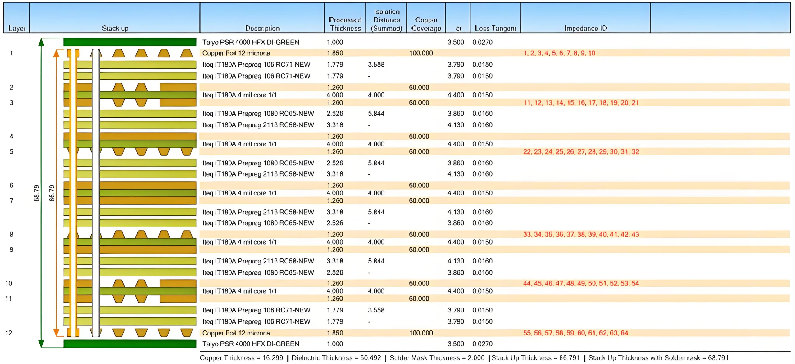
The core value of high-layer count PCBs lies in providing ample routing resources and complete reference planes. A typical 12-layer board stack-up might be: สัญญาณ 1 / พื้น / สัญญาณ 2 / พลัง 1 / สัญญาณ 3 / พื้น / สัญญาณ 4 / พลัง 2 / สัญญาณ 5 / พื้น / สัญญาณ 6. This symmetrical “ground-signal-power-signal-ground” stack-up (following guidelines like IPC-2141A) effectively controls impedance and provides a low-noise return path for high-speed signals. Statistics show that in equipment like data center switches, designs using PCBs with 20+ layers can reduce crosstalk in critical network signals by over 60% (data referenced from IPC TR-579 report).

Design Challenges for High-Layer Count PCBs: Beyond “Drawing Traces”
Signal Integrity and Impedance Control
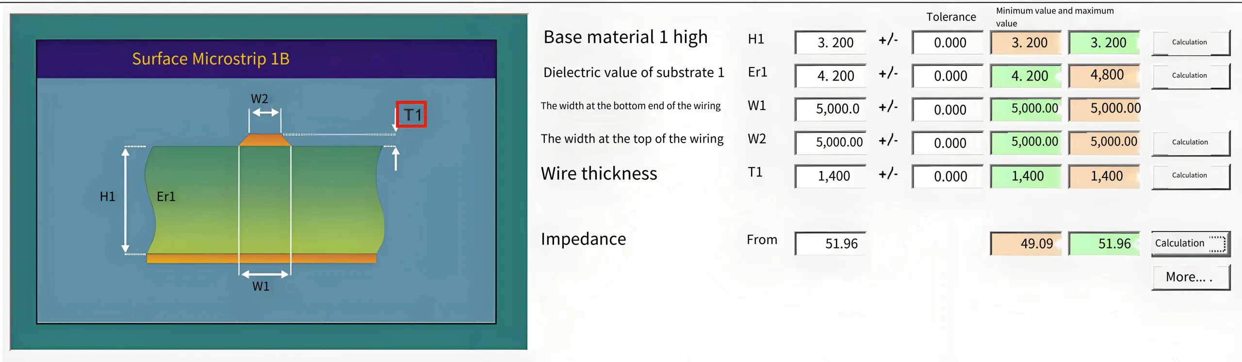
In high-speed design, PCB traces are no longer simple electrical connections but must be precisely controlled transmission lines. Deviations in characteristic impedance (เช่น, 50Ω single-ended, 90Ω/100Ω differential) directly cause signal reflection, overshoot, and data eye diagram closure. Impedance primarily depends on trace width (W), ความหนาอิเล็กทริก (ชม), ค่าคงที่ไดอิเล็กตริก (εr), and copper thickness. Industry-standard tools like Polar Si9000 model this using simplified formulas (for microstrip lines):
Z0 ≈ (87 / √(εr + 1.41)) * ln(5.98 * H / (0.8 * W + T))
where T is trace thickness. For common FR-4 material (εr ≈ 4.2 @ 1GHz), to achieve 50Ω impedance with a dielectric thickness H=5 mil, the trace width W needs to be controlled at approximately 8.5 MIL. อย่างไรก็ตาม, non-uniformity in the laminated structure of high-layer count boards, the glass weave effect, and production etching tolerances (typically ±10%) all introduce impedance variations. The IPC-6012D standard allows a ±10% deviation of the measured value from the nominal impedance for controlled impedance boards, but high-end applications now demand tolerances as tight as ±7%.

Power Integrity and PCB Thermal Management
As layer count increases, the complexity of Power Distribution Network (PDN) design grows exponentially. Core voltages can be as low as 0.8V with transient currents reaching hundreds of amps. In this scenario, the target impedance of the power planes must be extremely low (เช่น, <1 MΩ) to suppress voltage ripple. This requires careful planning of decoupling capacitor placement, optimization of inter-plane capacitance between power and ground planes (calculated by C = ε0 * εr * A / d, where A is the overlapping area and d is the dielectric thickness), and may necessitate dedicated power layers. นอกจากนี้, increased power density due to high-density routing (เกิน 100 W/cm² in some ASIC areas) requires enhanced cooling through thermal via arrays, embedded copper coins, or metal substrates, adding further complexity to stack-up design and processing.
The Alchemy of PCB Manufacturing: The Precision Process Chain for High-Layer Count Boards
Transforming design into physical reality presents another significant challenge for high-layer count PCBs. The core process can be summarized as a precise cycle of “lamination – alignment – drilling – plating.”
Layer-to-Layer Alignment: The Art of Micron-Level Registration
All layers of a multilayer board (inner layer cores and prepreg) must be laminated into a single unit under high temperature and pressure. Layer misregistration can cause drills to cut off traces, create shorts, or cause impedance discontinuities. For a 16-layer board, if the mean alignment error per layer is 25 μm (the graphic registration tolerance allowed by IPC-A-600G Class 3), the worst-case cumulative error could exceed 100 μm—enough to compromise a 0.2 mm BGA pad.
Leading manufacturers like UGPCB tackle this challenge using การถ่ายภาพโดยตรงด้วยเลเซอร์ (LDI) และ high-precision optical alignment systems. Alignment pins และ global fiducial scales etched on each core layer, combined with CCD vision capture and servo adjustment, can control layer-to-layer registration within 15 μm (data based on leading industry vendor process whitepapers). นอกจากนี้, material rheology analysis to predict resin flow and glass fiber orientation of prepreg during lamination allows for pre-compensation of dimensional deformation, ensuring uniform dielectric thickness after pressing.
https://example.com/pcb-lamination-alignment.png
Image Alt Text: Detailed explanation of multilayer PCB lamination and alignment process, showing laser targets, optical alignment, and lamination flow, ensuring high-precision layer-to-layer registration.
Via Interconnection: From Through-Holes to Any-Layer HDI
Traditional through-holes penetrate the entire board thickness, occupying significant routing space in high-layer count PCBs and causing long signal return path problems. ดังนั้น, การเชื่อมต่อระหว่างกันที่มีความหนาแน่นสูง (HDI) เทคโนโลยี enables more flexible layer transitions using จุดอ่อนตาบอด (from surface to inner layer), buried vias (inner layer to inner layer), และ microvias (diameter ≤ 0.15 มม).
ตัวอย่างเช่น, a “1+N+1” HDI structure (where surface layers use microvias and the middle is an N-layer traditional core) can increase routing density by over 40% without increasing total layer count (referencing IPC-2226 HDI design standard). อย่างไรก็ตาม, this introduces process complexities like sequential lamination drilling, via filling and plating, และ multiple lamination cycles. Manufacturers must equip laser drilling machines (for microvias), vertical vacuum plugging machines (to ensure void-free filling), และ plasma cleaning equipment (to remove drill smear), and perform rigorous flying probe testing และ four-wire Kelvin testing to verify the reliability of every interconnection point.
แนวโน้มในอนาคต: Material Innovation and Simulation-Driven Design-Manufacturing Integration
The evolution of high-layer count PCBs continues. As signal rates advance towards 56Gbps and beyond using PAM4 modulation, low-loss materials (like Panasonic MEGTRON 6, ซีรีส์ Rogers RO4000) with εr as low as 3.2 และปัจจัยการกระจาย (ฟ) ด้านล่าง 0.002 are being adopted. พร้อมกัน, embedded components (like buried resistors and capacitors) และ semiconductor package integration (เช่น, Intel’s EMIB, TSMC’s SoIC) are blurring the lines between PCBs and ICs.
For designers and procurement specialists, selecting a qualified high-layer count PCB supplier is paramount. Beyond focusing on their maximum layer capability (เช่น, stable mass production of 32 ชั้น), การควบคุมความต้านทาน ความสามารถ (whether they provide impedance test reports), และ HDI process level (minimum hole size/trace width), it is crucial to evaluate their design support services (such as SI/PI simulation and stack-up optimization advice) และ quality control system (adherence to IPC Class 3 standards and availability of comprehensive inspection equipment like AOI, AVI, 3D X-ray).

Seeking a high-reliability, ประสิทธิภาพสูง PCB หลายชั้น สารละลาย? Contacting a professional supplier with full-chain capabilities from design simulation to precision manufacturing to obtain a custom stack-up design proposal และ instant quote for your project is the first critical step toward success. In the era of the Internet of Everything and computational explosion, high-layer count PCBs are no longer just carriers; they are the foundational cornerstone defining the performance limits of electronic systems.