
ในอุตสาหกรรมอิเล็กทรอนิกส์ที่มีการพัฒนาอย่างรวดเร็วในปัจจุบัน, ที่ แผงวงจรพิมพ์ (พีซีบี) ทำหน้าที่เป็นกระดูกสันหลังของอุปกรณ์อิเล็กทรอนิกส์, ด้วยคุณภาพการออกแบบที่เป็นตัวกำหนดประสิทธิภาพของผลิตภัณฑ์โดยตรง, ความน่าเชื่อถือ, และค่าใช้จ่าย. ตามสถิติอุตสาหกรรม, เกือบ 40% ความล้มเหลวของแผงวงจรเกิดจากการกำกับดูแลในระหว่างขั้นตอนการออกแบบ, มากกว่าข้อบกพร่องด้านวัสดุหรือกระบวนการ (ตามที่รายงานไว้ในมาตรฐาน IPC-2221). คู่มือมืออาชีพนี้จะเจาะลึกหกหลัก การออกแบบ PCB เทคนิค, สอดคล้องกับเผด็จการ มาตรฐาน IPC, เพื่อช่วยให้ผู้ปฏิบัติงานก้าวหน้าจากระดับเริ่มต้นไปสู่ระดับผู้เชี่ยวชาญ. โดยการเรียนรู้วิธีการเหล่านี้, คุณสามารถประสบความสำเร็จในการออกแบบรอบแรกได้, ลดค่าใช้จ่ายในการผลิต, และเพิ่มความสามารถในการแข่งขันในตลาด—เหมาะอย่างยิ่งสำหรับการเพิ่มประสิทธิภาพการออกแบบ PCB และ แอสเซมบลี PCBA กระบวนการ.

ตำแหน่งส่วนประกอบ: เค้าโครงทางวิทยาศาสตร์เพื่อเพิ่มความสามารถในการผลิตและประสิทธิภาพการประกอบ
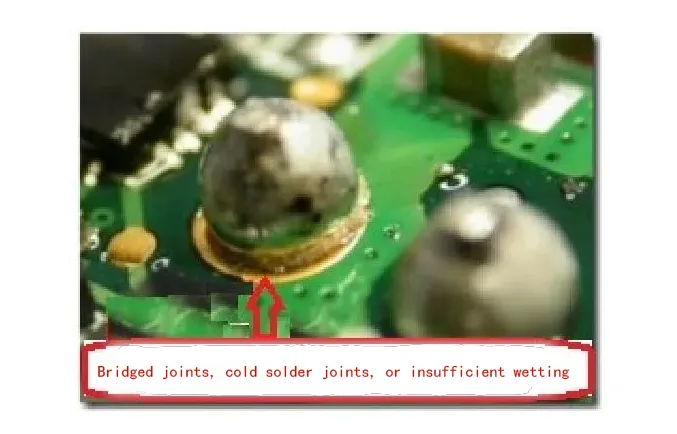
การจัดวางส่วนประกอบเป็นรากฐานของการออกแบบ PCB, ไม่เพียงส่งผลต่อประสิทธิภาพของวงจรเท่านั้น แต่ยังส่งผลต่อประสิทธิภาพการผลิตด้วย. นักออกแบบมือใหม่หลายคนให้ความสำคัญกับความเรียบร้อยของการมองเห็น แต่มองข้ามปัญหาต่างๆ เช่น ข้อต่อบัดกรีเย็น และการวางแนวที่ไม่ตรงระหว่างการประกอบ PCBA.
การวางแนวแบบรวมช่วยเพิ่มประสิทธิภาพกระบวนการบัดกรี
วางเฉย ส่วนประกอบ เช่น ตัวต้านทานและตัวเก็บประจุในทิศทางที่สม่ำเสมอ ช่วยลดเวลาที่ต้องใช้ในการปรับเครื่องจักรแบบหยิบและวางได้อย่างมาก. ตามแนวทาง IPC-2221, การวางแนวส่วนประกอบที่สอดคล้องกันสามารถเพิ่มประสิทธิภาพการบัดกรีได้มากกว่า 15% และลดอัตราข้อบกพร่องของข้อต่อบัดกรีเย็นให้ต่ำกว่า 5% (ข้อมูลที่มาจาก IPC-A-610, มาตรฐานการยอมรับของส่วนประกอบอิเล็กทรอนิกส์). ตัวอย่างเช่น, ส่วนประกอบโพลาไรซ์ทั้งหมด เช่น ไดโอด ควรหันไปในทิศทางเดียวกันเพื่อป้องกันข้อผิดพลาดในการกลับด้านในระหว่างการผลิต.
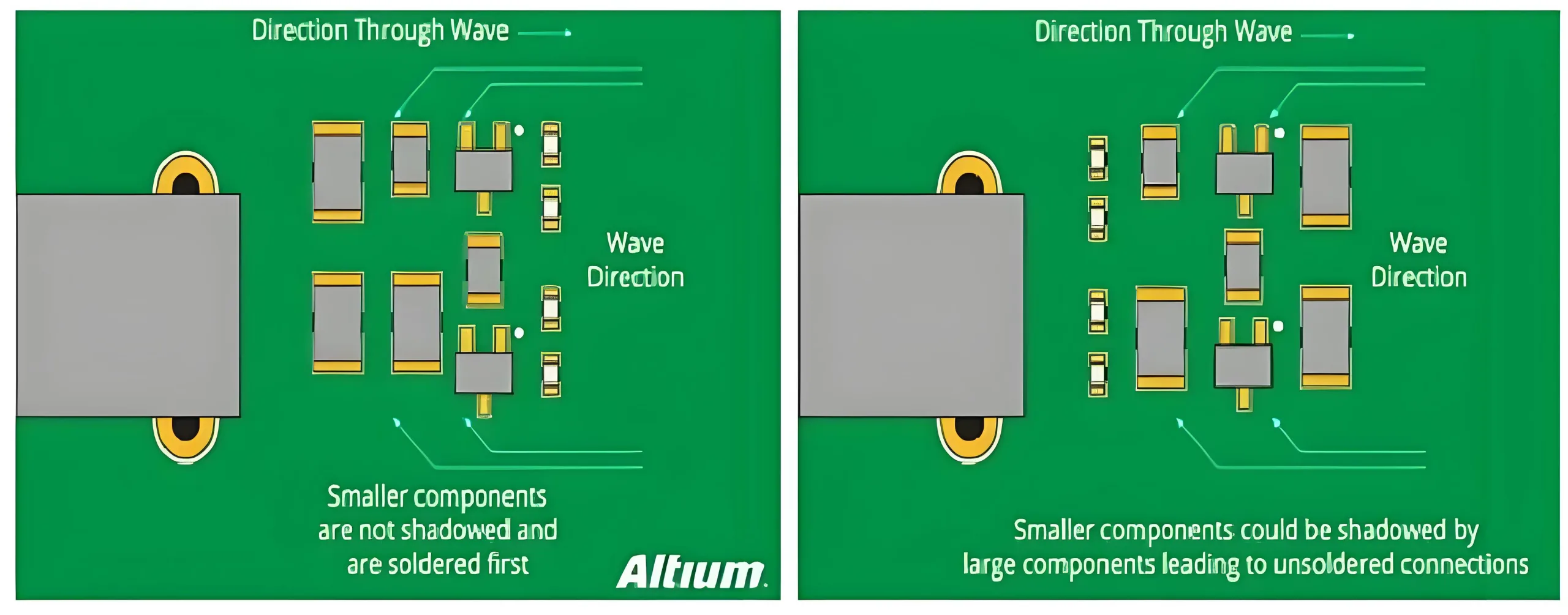
หลีกเลี่ยงเอฟเฟกต์การแรเงาของส่วนประกอบ
เมื่อส่วนประกอบมีขนาดเล็ก (เช่น, 0402 ตัวต้านทานแพ็คเกจ) ถูกวางไว้ใต้อันที่ใหญ่กว่าโดยตรง (เช่น, ตัวเก็บประจุด้วยไฟฟ้า), they create “shadow zones” that hinder proper solder wetting. การวิจัยระบุว่าพื้นที่ที่ไม่มีการขายในบริเวณที่มีร่มเงาสามารถเกิดขึ้นได้มากถึง 30% ของกรณี (อ้างถึง IPC-7095A). เพื่อให้แน่ใจว่าการบัดกรีไหลสม่ำเสมอ, รักษาระยะห่างขั้นต่ำระหว่างส่วนประกอบขนาดเล็กและขนาดใหญ่อย่างน้อย 1.5 คูณความสูงของส่วนประกอบที่เล็กกว่า.

กลยุทธ์การแยกส่วนประกอบ SMT และ Through-Hole
เทคโนโลยี Mount Surface (SMT) ส่วนประกอบควรเน้นที่ด้านหนึ่งของกระดาน, ในขณะที่ทะลุผ่านรู (ไทย) ควรวางส่วนประกอบไว้ที่ชั้นบนสุด. การจัดเรียงแบบแบ่งหมวดหมู่นี้จะช่วยลดจำนวนการพลิกบอร์ดระหว่างการประกอบ, อาจลดต้นทุนการประกอบโดย 20% ตามที่ประมาณไว้ตาม IPC-2222. สำหรับการออกแบบเทคโนโลยีผสม, ประเมินขั้นตอนเพิ่มเติม เช่น การคัดเลือกการเชื่อมล่วงหน้า และร่วมมือกับผู้มีประสบการณ์ ผู้ผลิต PCB และซัพพลายเออร์ PCBA เช่น UGPCB เพื่อรับรองคุณภาพและความน่าเชื่อถือของผลิตภัณฑ์ในการผลิตและการประกอบ PCB.
การออกแบบเส้นทาง PCB: มั่นใจในเสถียรภาพด้านพลังงาน, พื้น, และร่องรอยสัญญาณ
การออกแบบเส้นทางส่งผลโดยตรงต่อประสิทธิภาพทางไฟฟ้า; รูปแบบที่ไม่เหมาะสมอาจส่งผลให้ความสมบูรณ์ของสัญญาณลดลง, เสียงของแหล่งจ่ายไฟเพิ่มขึ้น, หรือแม้กระทั่งความล้มเหลวจากความร้อนสูงเกินไป. การปฏิบัติตามมาตรฐาน IPC ช่วยลดความเสี่ยงเหล่านี้ได้อย่างมีประสิทธิภาพ.
เค้าโครงชั้นในสำหรับระนาบกำลังและกราวด์
การวางตำแหน่งกำลังและระนาบกราวด์ด้านใน ชั้น PCB ด้วยการกระจายแบบสมมาตรป้องกันการบิดเบี้ยวของบอร์ด. อ้างอิงจาก IPC-2141, วิธีการออกแบบนี้จะจำกัดความแปรผันของอิมพีแดนซ์ไว้ภายใน 10%, เพิ่มความเสถียรในการส่งสัญญาณความถี่สูง. สำหรับการส่งกำลังของชิป, แนะนำให้ใช้โทโพโลยีแบบดาวมากกว่าการเชื่อมต่อแบบเดซี่เชน, และความกว้างของการติดตามจะต้องคำนวณตามกระแส: ตัวอย่างเช่น, ใช้สูตร IPC-2221 สำหรับความกว้างการติดตามขั้นต่ำ:
ผม = k × ΔT^0.44 × A^0.725
ที่ฉันอยู่ในปัจจุบัน (อัน), ∆T คืออุณหภูมิที่เพิ่มขึ้น (องศาเซลเซียส), A เป็นพื้นที่หน้าตัด (ล้าน²), และ k เป็นค่าคงที่ (0.024 สำหรับชั้นนอก). สมมติว่า ΔT=10°C, กระแสไฟ 1A ต้องการความกว้างการติดตามอย่างน้อย 20 มิลลิลิตรเพื่อป้องกันความร้อนสูงเกินไป.
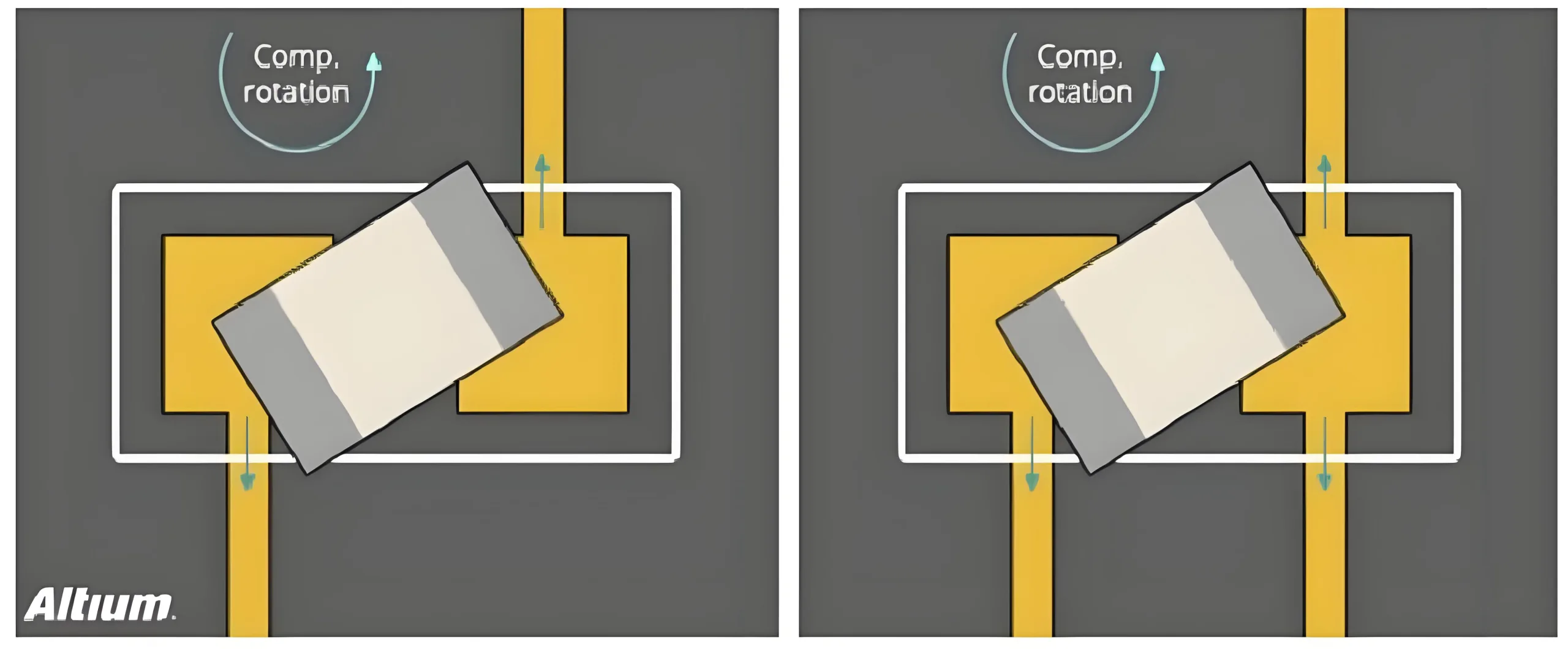
หลักการเส้นทางที่สั้นที่สุดสำหรับการติดตามสัญญาณ
การติดตามสัญญาณควรเป็นไปตามระยะสั้น, เส้นทางตรงเพื่อลดการเหนี่ยวนำและความจุของปรสิต. สำหรับส่วนประกอบคงที่ในแนวนอน, ติดตามเส้นทางในแนวนอนก่อนที่จะทำการเลี้ยวในแนวตั้งเพื่อป้องกันการวางแนวที่ไม่ตรงที่เกิดจากการไหลของบัดกรี. IPC-2221 ตั้งข้อสังเกตว่าเทคนิคนี้สามารถลดความล่าช้าของสัญญาณได้ด้วย 15% และลดการรบกวนทางแม่เหล็กไฟฟ้า (อีเอ็มไอ), สำคัญมากสำหรับ การออกแบบ PCB ความเร็วสูง และความสมบูรณ์ของสัญญาณ.

การจับคู่ความกว้างของการติดตาม PCB กับโหลดปัจจุบัน
สัญญาณกระแสต่ำ (เช่น, สัญญาณดิจิตอล/อนาล็อก) สามารถใช้ความกว้างการติดตาม 10mil, แต่ต้องเพิ่มความกว้างสำหรับกระแสเกิน 0.3A. ตัวอย่างเช่น, กระแสไฟ 3A ต้องมีความกว้างอย่างน้อย 50mil (คำนวณตาม IPC-2221). การเพิกเฉยกฎนี้อาจนำไปสู่อุณหภูมิการติดตามที่เพิ่มขึ้นมากเกินไปและความล้มเหลวของวงจรเปิด, เน้นย้ำถึงความสำคัญของรูปแบบ PCB ที่แข็งแกร่งเพื่อความสมบูรณ์ของพลังงาน.
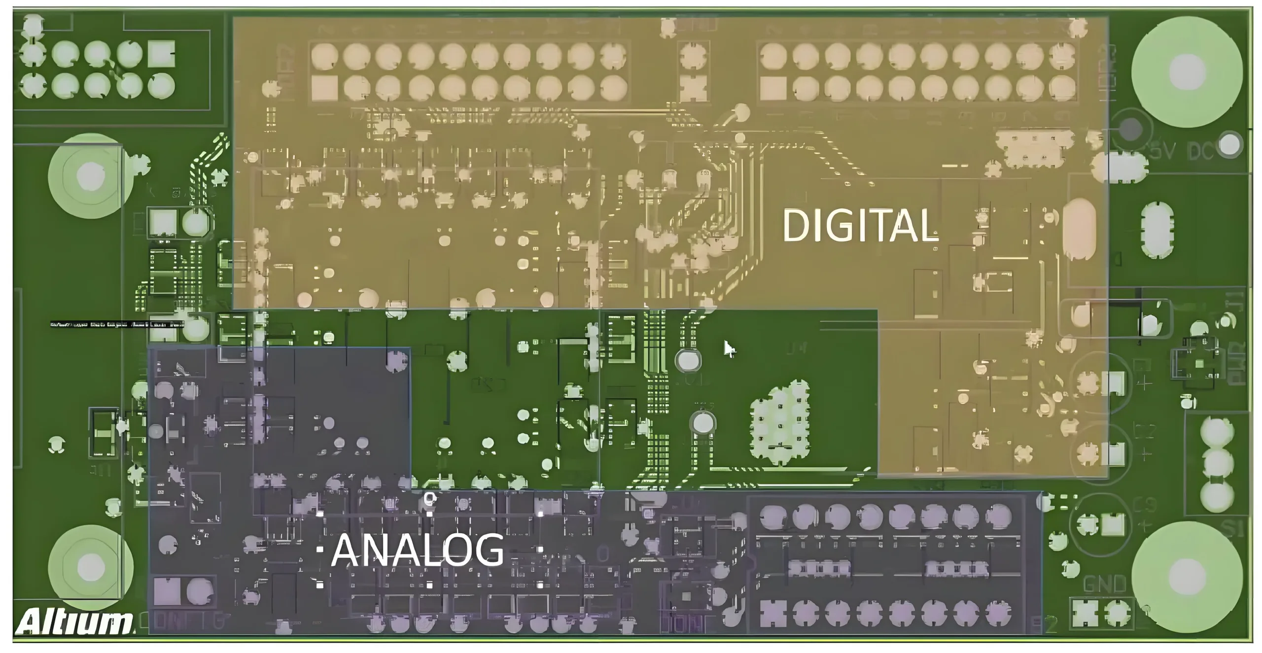
การออกแบบแยก: กลยุทธ์ป้องกันการรบกวนสำหรับดิจิทัล, อนาล็อก, และวงจรไฟฟ้า
ในวงจรสัญญาณผสม, สัญญาณรบกวนการสลับอย่างรวดเร็วจากวงจรดิจิตอลสามารถรบกวนวงจรอะนาล็อกที่มีความละเอียดอ่อนได้อย่างง่ายดาย, ทำให้เกิดการบิดเบือนของสัญญาณ. การแยกทางกายภาพและทางไฟฟ้าช่วยเพิ่มอัตราส่วนสัญญาณต่อเสียงรบกวนของระบบได้อย่างมาก.
แยกกราวด์กำลังและกราวด์ควบคุม
เดินสายกราวด์กลับคืนสำหรับแหล่งจ่ายไฟแต่ละตัวโดยแยกจากกัน, เชื่อมต่อไว้ที่จุดเดียวเท่านั้นที่ปลายเส้นทางไฟฟ้า. ตามแนวทาง IPC-2221, การออกแบบนี้สามารถเพิ่มการปฏิเสธเสียงรบกวนในโหมดทั่วไปได้มากกว่า 60dB. ตัวอย่างเช่น, ในการควบคุมมอเตอร์ PCBS, แยกกราวด์ตัวขับมอเตอร์ออกจากกราวด์ควบคุม MCU เพื่อหลีกเลี่ยงสัญญาณรบกวน.
การแบ่งพาร์ติชันวงจรดิจิตอลและอนาล็อกอย่างเข้มงวด
วงจรดิจิทัลแยกทางกายภาพ (เช่น, MCU) จากวงจรอนาลอก (เช่น, เซ็นเซอร์), และแยกระนาบกราวด์ออกเป็นส่วนต่าง ๆ ที่เชื่อมต่อกันผ่านเส้นทางอิมพีแดนซ์ที่ควบคุมเท่านั้น. IPC-2251 แนะนำระยะห่างขั้นต่ำ 50 มิลลิเมตร และจำกัดการติดตามสัญญาณอนาล็อกเหนือระนาบกราวด์อนาล็อกอย่างเคร่งครัด. ข้อมูลการทดสอบแสดงให้เห็นว่าวิธีนี้สามารถลดการรบกวนของการเชื่อมต่อแบบ capacitive ได้ด้วย 70%, สำคัญสำหรับการออกแบบ PCB สัญญาณผสม.

การจัดการความร้อน: การจัดการความร้อนอย่างมีประสิทธิภาพเพื่อยืดอายุการใช้งานของแผงวงจร
ความร้อนเป็นสาเหตุหลักของความล้มเหลวของชิ้นส่วนอิเล็กทรอนิกส์, โดยเฉพาะในการใช้งานที่มีกำลังสูง. การออกแบบการระบายความร้อนที่ไม่เพียงพออาจทำให้ประสิทธิภาพลดลงหรือเกิดความเสียหายถาวรได้, การเพิ่มประสิทธิภาพที่จำเป็นตามพารามิเตอร์ความต้านทานความร้อน.
ระบุส่วนประกอบต้านทานความร้อนสูง
ศึกษาเอกสารข้อมูลส่วนประกอบสำหรับการต้านทานความร้อน (θJA); ตัวอย่างเช่น, ตัวควบคุม LDO ที่มี θJA=50°C/W พบกับอุณหภูมิที่เพิ่มขึ้น 50°C ต่อวัตต์ของการกระจายพลังงาน. วางส่วนประกอบที่มีกำลังสูง (เช่น, MOSFET) ห่างจากอุปกรณ์ที่ไวต่ออุณหภูมิ และรวมแผงระบายความร้อนหรือพัดลมไว้ด้วย. IPC-2221 แนะนำระยะห่างขั้นต่ำระหว่างส่วนประกอบกำลังอย่างน้อยสองเท่าของความกว้างของส่วนประกอบเพื่อส่งเสริมการหมุนเวียนอากาศ.
การใช้แผ่นระบายความร้อน
สำหรับส่วนประกอบของรูทะลุ, แผ่นระบายความร้อนมีความสำคัญอย่างยิ่งในการป้องกันข้อบกพร่องในการบัดกรี. พวกเขาเชื่อมต่อแผ่นอิเล็กโทรดกับพื้นที่ทองแดงขนาดใหญ่ผ่านซี่ทองแดงแคบ, ชะลอการกระจายความร้อน. อ้างอิงจาก IPC-7351, แผ่นระบายความร้อนสามารถปรับปรุงความสม่ำเสมอของอุณหภูมิการบัดกรีได้โดย 25%, ลดความเสี่ยงของข้อต่อประสานเย็น.
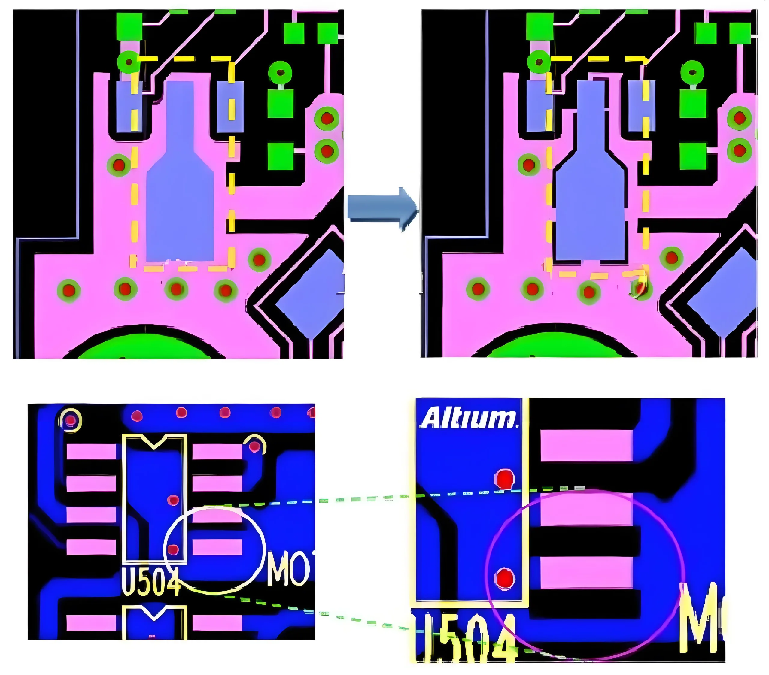

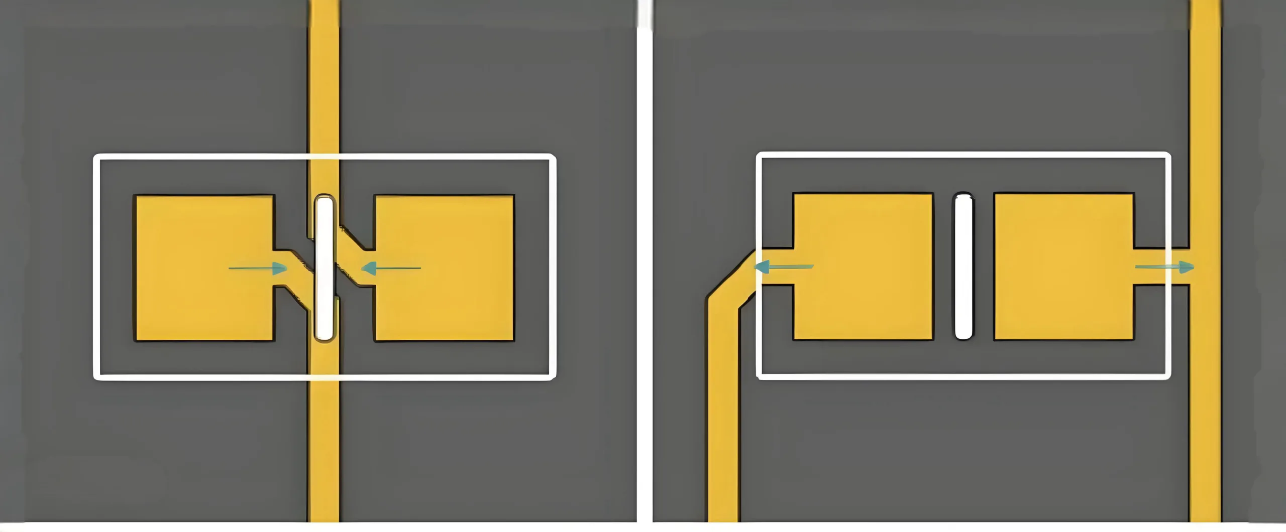
แผ่นระบายความร้อน: วิธีแก้ปัญหาระดับมืออาชีพสำหรับข้อบกพร่องในการบัดกรี
มักถูกมองข้ามโดยมือใหม่, แผ่นระบายความร้อนมีบทบาทสำคัญในการป้องกันปัญหาต่างๆ เช่น การไม่เปียกและการบัดกรีหลอก. เมื่อแผ่นอิเล็กโทรดขนาดเล็กเชื่อมต่อกับบริเวณทองแดงขนาดใหญ่, การสูญเสียความร้อนอย่างรวดเร็วสามารถป้องกันไม่ให้บัดกรีละลายได้อย่างถูกต้อง.
หลักการทำงานและสูตรการออกแบบ
แผ่นระบายความร้อนช่วยรักษาอุณหภูมิการบัดกรีโดยการลดพื้นที่การนำความร้อน. การอ้างอิงการออกแบบจาก IPC-2221 แนะนำให้ใช้ซี่ล้อเชื่อมต่อโดยทั่วไปสี่ซี่, แต่ละอันมีความกว้างประมาณ 20% ของเส้นผ่านศูนย์กลางแผ่น. ตัวอย่างเช่น, แป้นขนาด 40 มิลจะใช้ซี่ล้อกว้าง 8 มิล, ปรับสมดุลการนำไฟฟ้าและการแยกความร้อน. การทดลองระบุว่าการออกแบบนี้สามารถเพิ่มอัตราความสำเร็จในการบัดกรีได้มากกว่า 95%.

การตรวจสอบการออกแบบ: การตรวจสอบขั้นสุดท้ายเพื่อให้แน่ใจว่าไม่มีข้อบกพร่อง
หลังจากการออกแบบเสร็จสิ้น, การตรวจสอบอย่างเป็นระบบทำหน้าที่เป็นด่านสุดท้ายในการป้องกันความล้มเหลวของแบทช์. การใช้เครื่องมือซอฟต์แวร์ออกแบบ PCB และการตรวจสอบโดยเจ้าหน้าที่สามารถตรวจพบข้อผิดพลาดที่อาจเกิดขึ้นได้.
การตรวจสอบกฎไฟฟ้า (กกพ) และการตรวจสอบกฎการออกแบบ (ดีอาร์ซี)
เรียกใช้ ERC และ DRC เพื่อตรวจสอบพารามิเตอร์ เช่น ความกว้างของการติดตาม, ระยะห่าง, และไฟฟ้าลัดวงจร. ตัวอย่างเช่น, IPC-2221 ระบุระยะห่างการติดตามขั้นต่ำ 4mil สำหรับการใช้งานแรงดันไฟฟ้าต่ำ. เครื่องมือเช่น Altium Designer จะทำเครื่องหมายการละเมิดโดยอัตโนมัติ, ลดข้อผิดพลาดของมนุษย์.
การตรวจสอบสัญญาณต่อสัญญาณด้วยตนเอง
จากแผนผังไปจนถึงเค้าโครง PCB, ตรวจสอบการเชื่อมต่อสัญญาณแต่ละรายการแยกกันเพื่อให้แน่ใจว่าไม่มีลิงก์ที่พลาดหรือไม่ถูกต้อง. ใช้การไฮไลต์เพื่อแยกเครือข่ายที่สำคัญ, เช่น สัญญาณนาฬิกา, และตรวจสอบการเพิ่มประสิทธิภาพเส้นทาง. สถิติแสดงให้เห็นว่าวิธีนี้สามารถลดอัตราความผิดพลาดในการออกแบบได้ 80% (ข้อมูลจากแนวทางการตรวจสอบการออกแบบ IPC).
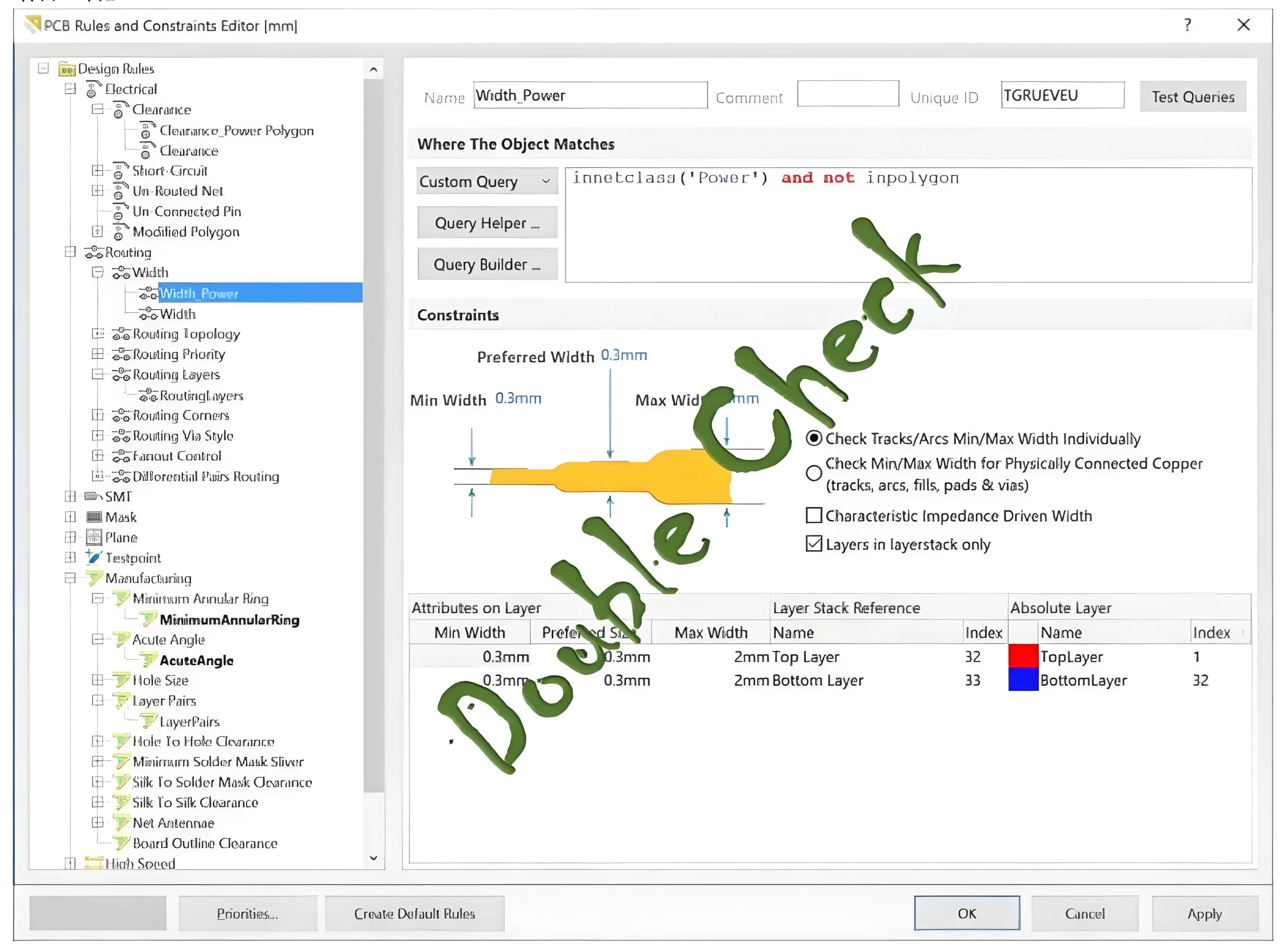

[ภาพ 6: DRC ตรวจสอบแผนผังอินเทอร์เฟซ]
Alt: ตัวอย่างอินเทอร์เฟซการตรวจสอบกฎการออกแบบ PCB ที่แสดงความกว้างของการติดตามและการตรวจสอบระยะห่าง, กุญแจสำคัญสำหรับการออกแบบ PCB ที่ปราศจากข้อผิดพลาดและความพร้อมของ PCBA.
บทสรุป
การออกแบบ PCB เป็นการผสมผสานทางวิศวกรรมและศิลปะเข้าด้วยกัน. โดยการเรียนรู้การจัดวางส่วนประกอบ, กลยุทธ์การกำหนดเส้นทาง, การออกแบบแยก, การเพิ่มประสิทธิภาพทางความร้อน, การใช้แผ่นระบายความร้อน, และการตรวจสอบอย่างเป็นระบบ, คุณสามารถเพิ่มความสามารถในการผลิตและความน่าเชื่อถือของบอร์ดได้อย่างมาก. ในฐานะผู้เริ่มต้น, มุ่งเน้นไปที่เทคนิคพื้นฐานเหล่านี้และทำซ้ำโครงการเชิงปฏิบัติเพื่อออกแบบ PCB ที่มีประสิทธิภาพสูง. หากคุณต้องการการสนับสนุนด้านการผลิต PCB/PCBA อย่างมืออาชีพ, ติดต่อทีมซัพพลายเออร์ของเราเพื่อประเมินการออกแบบฟรีและเสนอราคาเพื่อปกป้องโครงการของคุณ. จดจำ, การออกแบบที่ยอดเยี่ยมไม่เพียงแต่ช่วยลดต้นทุนเท่านั้น แต่ยังช่วยเพิ่มพลังให้กับนวัตกรรมอีกด้วย!