
การแนะนำ: บทบาทสำคัญของการควบคุมสิ่งแวดล้อมใน PCB/PCBA
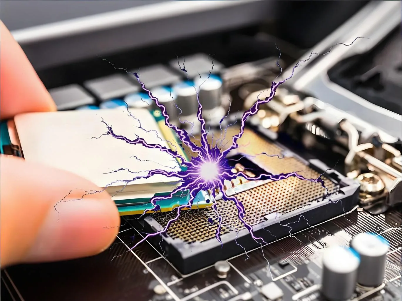
การปล่อยประจุไฟฟ้าสถิตเบาๆ สามารถทำลายไมโครโปรเซสเซอร์อันมีค่าได้ในทันที. คุณลืมบีจีเอ ส่วนประกอบ, สัมผัสกับอากาศชื้น, อาจออกซิไดซ์อย่างเงียบๆ, นำไปสู่ข้อบกพร่องในการบัดกรี. ภัยคุกคามที่ซ่อนอยู่เหล่านี้แสดงถึงความท้าทายด้านการจัดการสิ่งแวดล้อมที่สำคัญซึ่งไม่สามารถละเลยได้ การผลิต PCB.

ในอาณาจักรของ PCB และ พีซีบี การผลิต, การปล่อยไฟฟ้าสถิต (ESD) และอุปกรณ์ไวต่อความชื้น (กระทรวงสาธารณสุข) การจัดการเป็นปัจจัยสำคัญที่ส่งผลต่อความน่าเชื่อถือของผลิตภัณฑ์และผลผลิตที่ผ่านครั้งแรก. เนื่องจากอุปกรณ์อิเล็กทรอนิกส์มีแนวโน้มไปสู่การย่อขนาดและมีความหนาแน่นสูงขึ้น, ความเสี่ยงที่อาจเกิดขึ้นจาก ESD และส่วนประกอบที่ไวต่อความชื้นจะเด่นชัดยิ่งขึ้น.
ข้อมูลทางสถิติบ่งชี้ว่าจบแล้ว 60% ของเพลิงไหม้และเหตุการณ์ไฟฟ้าช็อตในระบบไฟฟ้าแรงต่ำมีสาเหตุมาจากความผิดปกติของสายดิน, โดยเฉพาะข้อผิดพลาดที่เกิดจากอาร์ค. นอกจากนี้, ประมาณ 30% ของอุบัติเหตุไฟฟ้าช็อตสัมพันธ์กับการไม่มี RCD (อุปกรณ์ตกค้างปัจจุบัน) หรือการเลือก RCD ไม่ถูกต้อง. การจัดการ ESD และ MSD อย่างมีประสิทธิผลเป็นพื้นฐานในการลดความเสี่ยงดังกล่าว พีซีบี การผลิต.
การป้องกัน ESD: จากหลักการพื้นฐานสู่การนำไปปฏิบัติจริง
การปล่อยไฟฟ้าสถิต (ESD) เป็นหัวข้อสำคัญภายในความเข้ากันได้ทางแม่เหล็กไฟฟ้า (EMC), โดยเฉพาะสำหรับอุปกรณ์อิเล็กทรอนิกส์ยุคใหม่ซึ่งเหตุการณ์ ESD อาจทำให้อุปกรณ์ทำงานผิดปกติได้, ข้อมูลสูญหาย, หรือความเสียหายของฮาร์ดแวร์ถาวร. การใช้มาตรการควบคุม ESD ที่มีประสิทธิภาพถือเป็นสิ่งสำคัญสำหรับผู้ผลิต PCB ที่จริงจัง.
กลไก ESD และแบบจำลองความเสียหาย
ESD ส่งผลกระทบต่ออุปกรณ์อิเล็กทรอนิกส์เป็นหลักผ่านกลไกสามประการ: เอฟเฟกต์การนำโดยตรงผ่าน I/O หรือพอร์ตจ่ายไฟ; ผลกระทบของการควบแน่นของสนามผ่านการมีเพศสัมพันธ์แบบแผ่รังสีใกล้สนาม; และผลกระทบของพัลส์แม่เหล็กไฟฟ้าจากการเปลี่ยนแปลงอย่างรวดเร็ว, การรบกวนทางแม่เหล็กไฟฟ้าบรอดแบนด์.
ภายในสภาพแวดล้อมการผลิต PCB, ESD มักเกิดขึ้นในโหมดการคายประจุสามโหมด:
-
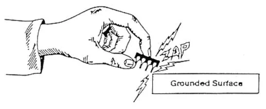
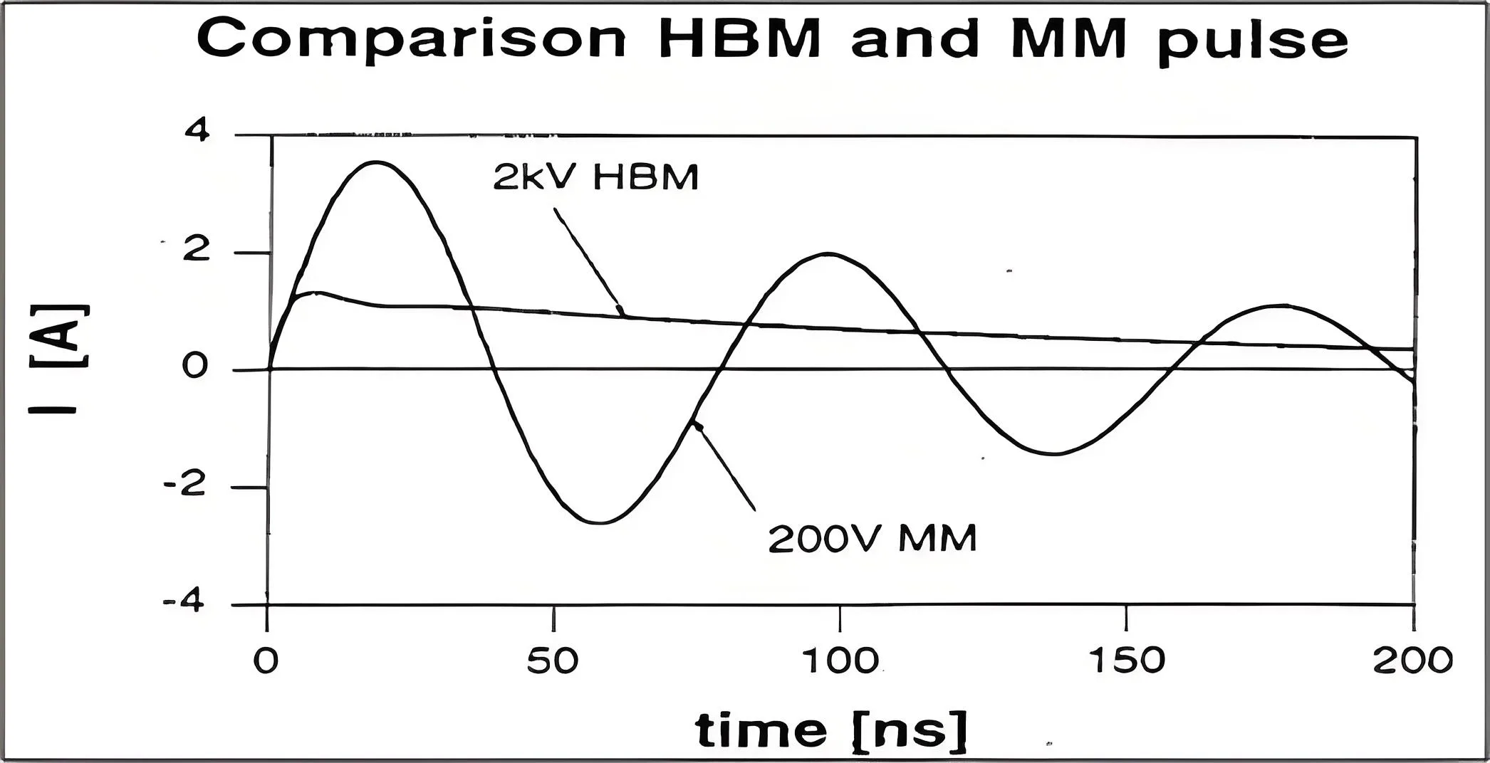
แบบจำลองร่างกายมนุษย์ (HBM): บุคคลสะสมประจุไฟฟ้าสถิตผ่านการเคลื่อนไหวหรือการเสียดสี. เมื่อสัมผัสวงจรรวม (ไอซี), ประจุไฟฟ้าสถิตที่เก็บไว้จะคายประจุผ่านหมุดของ IC ลงกราวด์. การคายประจุนี้สามารถสร้างกระแสไฟกระชากหลายแอมแปร์ภายในเวลาไม่กี่ร้อยนาโนวินาที.

-
รุ่นเครื่อง (มม.): เครื่องจักรเองก็สะสมประจุไฟฟ้าสถิต. เมื่อเครื่องสัมผัสกับไอซี, การปล่อยประจุไฟฟ้าสถิตเกิดขึ้นผ่านหมุดของ IC. เนื่องจากเครื่องจักรโดยทั่วไปมักเป็นโลหะ, ความต้านทานการคายประจุที่เท่ากันนั้นต่ำมาก, ส่งผลให้กระบวนการคายประจุเร็วขึ้นอีก—หลายแอมแปร์ภายในนาโนวินาทีถึงสิบนาโนวินาที.

-
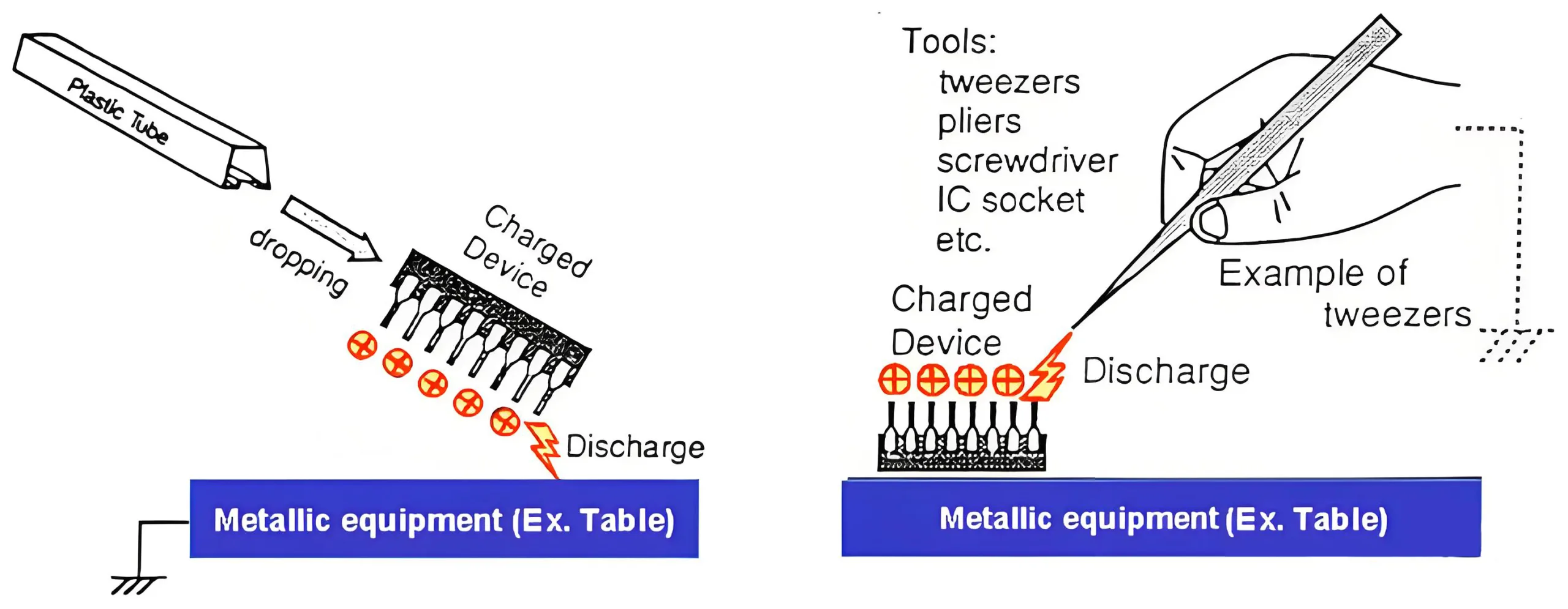
รุ่นอุปกรณ์ที่ชาร์จ (ซีดีเอ็ม): IC จะสะสมประจุไฟฟ้าสถิตภายในผ่านการเสียดสีหรือวิธีการอื่นๆ โดยไม่มีความเสียหายในทันที. ต่อมา, เมื่อพินของ IC ที่มีประจุสัมผัสกับพื้นผิวที่ต่อสายดิน, ประจุไฟฟ้าสถิตภายในจะไหลออกอย่างรวดเร็วผ่านพิน, ทำให้เกิดเหตุการณ์การปลดประจำการ.

วัสดุป้องกัน ESD และมาตรฐานการต่อสายดิน
การป้องกัน ESD ที่มีประสิทธิผลต้องอาศัยวัสดุที่เหมาะสมและวิธีการลงกราวด์ทางวิทยาศาสตร์. โลหะเป็นตัวนำและอาจสร้างความเสียหายให้กับส่วนประกอบเนื่องจากกระแสรั่วไหลสูง. ลูกถ้วยมีแนวโน้มที่จะเกิดการชาร์จแบบไทรโบอิเล็กทริก. ดังนั้น, โลหะบริสุทธิ์หรือฉนวนไม่ใช่วัสดุป้องกัน ESD ในอุดมคติ. แทน, วัสดุที่ใช้ได้แก่ตัวนำไฟฟ้าสถิต (ความต้านทานพื้นผิว < 1×10⁵ Ω·ซม) และวัสดุกระจายไฟฟ้าสถิต (ความต้านทานพื้นผิวระหว่าง 1×10⁵ Ω·cm และ 1×10⁸ Ω·cm).
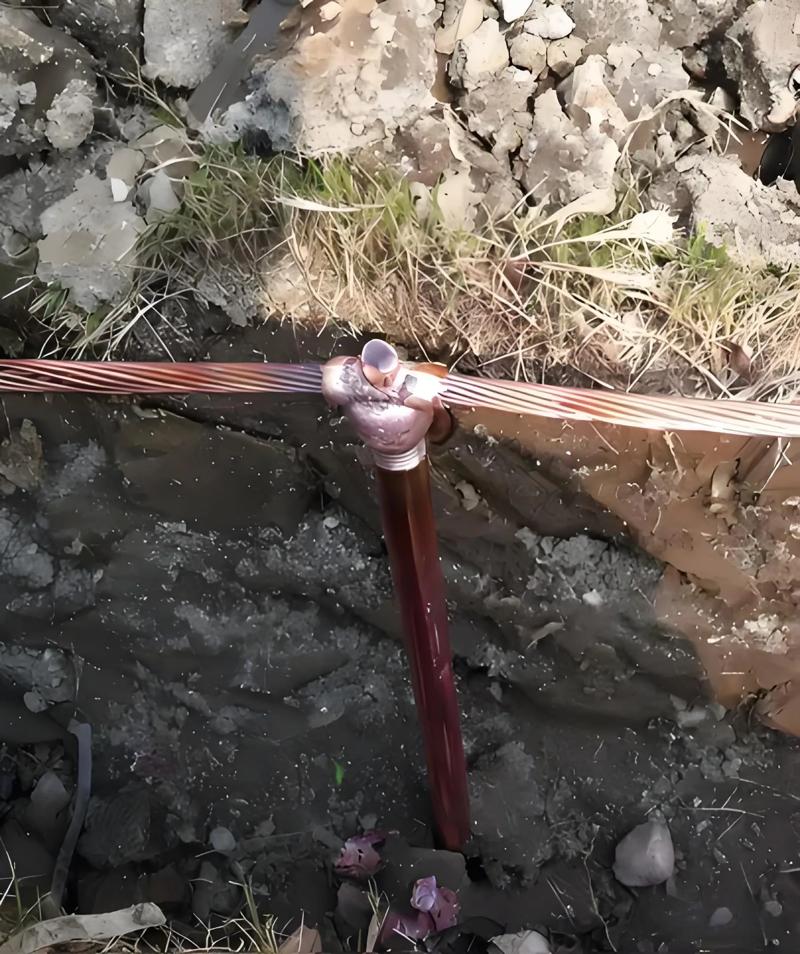
การต่อสายดินเป็นรากฐานสำคัญของการป้องกัน ESD. ตามมาตรฐานทั่วไป, โดยทั่วไปความต้านทานของอิเล็กโทรดกราวด์ ESD ควรน้อยกว่า 4Ω (ด้วยมาตรฐานบางอย่าง, เช่นเดียวกับมาตรฐานบางอย่างของสหรัฐอเมริกา, ต้องการ <1โอ้). ระบบสายดินที่แข็งแกร่งมักใช้วิธีการแบบหลายจุด: เว้นระยะห่างพื้นอย่างน้อยสามจุด 3-5 ห่างกันหลายเมตร, ใช้แท่งเหล็กหุ้มทองแดงขับเคลื่อนในแนวตั้ง 2 ลงไปในหลุมลึกกว่า 0.5 เมตร. จุดเหล่านี้ถูกเชื่อมเข้าด้วยกันด้วยตัวนำตีเกลียวขนาด 70 มม.², และลวดทองแดงหุ้มฉนวนขนาด 16 มม.² เชื่อมต่อจากโครงข่ายนี้กับภายในอาคารเป็นบัสกราวด์หลัก.
ข้อกำหนดด้านพื้นผิวการทำงานและพื้นที่การต่อลงดินมีความเข้มงวดมากยิ่งขึ้น: สายกราวด์ ESD ควรใช้ลวดทองแดงหุ้มฉนวนหลายเส้นขนาด 6 มม.², และความต้านทานระหว่างจุดทดสอบ ESD และกราวด์บัสหลัก ESD ควรรักษาไว้ภายใน 5-15Ω.
มาตรฐานและวิธีการทดสอบ ESD
คณะกรรมาธิการไฟฟ้าเทคนิคระหว่างประเทศ (IEC) มาตรฐานไออีซี 61000-4-2 ควบคุมภูมิคุ้มกันของอุปกรณ์อิเล็กทรอนิกส์ต่อ ESD. ที่ 2025 edition นำเสนอข้อกำหนดด้านภูมิคุ้มกันที่เข้มงวดยิ่งขึ้น และวิธีการทดสอบ/พารามิเตอร์ที่ได้รับการปรับปรุงใหม่ เพื่อตอบสนองความต้องการของอุปกรณ์อิเล็กทรอนิกส์รุ่นใหม่.
การทดสอบ ESD จะดำเนินการในสองโหมดเป็นหลัก: ติดต่อ Discharge และ Air Discharge. การคายประจุแบบสัมผัสเป็นการจำลองการสัมผัสโดยตรงระหว่างผู้ใช้/วัตถุและอุปกรณ์, ด้วยแรงดันทดสอบทั่วไปที่ 8kV. การระบายอากาศจะจำลองประกายไฟที่ไม่สัมผัสจากผู้ใช้/วัตถุที่มีประจุซึ่งเข้าใกล้อุปกรณ์, ด้วยแรงดันทดสอบทั่วไปที่ 15kV.
(H3) ระดับการทดสอบ ESD ตาม IEC 61000-4-2 มาตรฐาน
| ระดับการทดสอบ | ติดต่อจำหน่าย (KV) | การระบายอากาศ (KV) |
|---|---|---|
| 1 | 2 | 2 |
| 2 | 4 | 4 |
| 3 | 6 | 8 |
| 4 | 8 | 15 |
อุปกรณ์ไวต่อความชื้น (กระทรวงสาธารณสุข) การจัดการ: ควบคุมได้อย่างสมบูรณ์ตั้งแต่การระบุตัวตนไปจนถึงการอบขนม
การจัดการ MSD เป็นอีกหนึ่งองค์ประกอบการควบคุมที่สำคัญ SMT สภาพแวดล้อม. Improper humidity control can lead to the “popcorn effect” during reflow soldering, โดยที่ความชื้นภายในระเหยอย่างรวดเร็ว, ทำให้เกิดการหลุดร่อนและรอยแตกร้าวภายในส่วนประกอบ.
การระบุและการจำแนก MSD
อุปกรณ์ที่ไวต่อความชื้นเป็นส่วนประกอบที่ไวต่อความเสียหายจากความชื้น, รวมถึง PCB และ IC เป็นหลัก (เช่น, BGA, MF). แบ่งออกเป็นแปดระดับ (1, 2, 2อัน, 3, 4, 5, 5อัน, 6), แต่ละประเภทมีข้อกำหนดอายุพื้นที่เฉพาะเจาะจง.
อายุการใช้งานหมายถึงเวลาที่ยอมให้ MSD สัมผัสกับสภาพพื้นโรงงานหลังจากเปิดถุงปิดผนึกแล้ว. มีตั้งแต่ 1 ปี (ระดับ 2) ที่ต้องอบทันทีก่อนใช้งาน (ระดับ 6). การระบุและการจำแนกประเภทที่ถูกต้องเป็นข้อกำหนดเบื้องต้นสำหรับการจัดการที่มีประสิทธิผล.
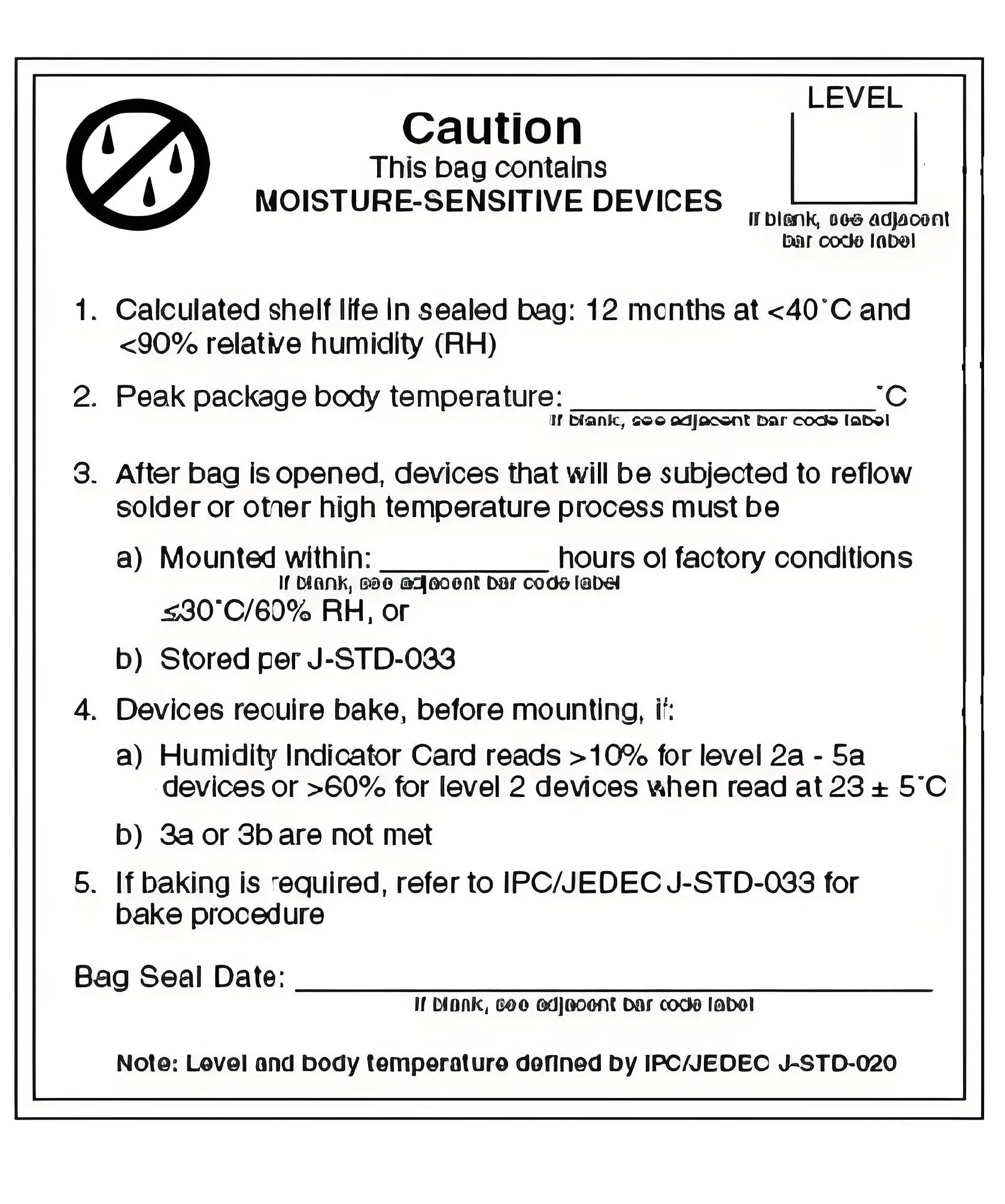

ข้อมูลจำเพาะด้านการจัดเก็บและการจัดการ MSD
สภาพแวดล้อมการจัดเก็บข้อมูลสำหรับ MSD จำเป็นต้องมีการควบคุมที่เข้มงวด. อุณหภูมิคลังสินค้าควรอยู่ที่ ≤30°C, โดยมีการควบคุมความชื้นระหว่าง ≤85%RH ถึง ≤70%RH ขึ้นอยู่กับระดับ MSD.
ข้อกำหนดด้านบรรจุภัณฑ์แตกต่างกันไปตามระดับ: ระดับ 1-2a ไม่มีข้อกำหนดพิเศษ; ระดับ 3-5a ต้องใช้ถุงป้องกันความชื้น, สารดูดความชื้น, และป้ายเตือน; ระดับ 6 ต้องมีป้ายเตือน แต่ไม่มีถุงกั้นความชื้น.
เมื่อเปิดแล้ว, ต้องใช้ MSD อย่างเคร่งครัดภายในอายุพื้นที่ระบุไว้. เจ้าหน้าที่ฝ่ายผลิตควรกำหนดปริมาณที่จะเปิดตามกำหนดการผลิต. ทันทีที่เปิด, an “MSD Component Control Card” must be attached. ส่วนประกอบใดๆ ที่ไม่ได้ใช้ทันทีควรเก็บไว้ในตู้แห้งชั่วคราว (25±5°ซ, ≤30% ความชื้น).
ขั้นตอนการอบ MSD
จำเป็นต้องอบเมื่อ MSD เกินเวลาเปิดรับแสงที่อนุญาต หรือเมื่อการ์ดตัวบ่งชี้ความชื้น (เอชไอซี) แสดงระดับความชื้นเกินมาตรฐาน (เช่น, >30%RH). การอบเป็นสิ่งจำเป็นภายใต้เงื่อนไขเหล่านี้:
-
บรรจุภัณฑ์สูญญากาศที่เข้ามาเสียหายหรือรั่ว.
-
HIC แสดงความชื้นเกิน 30%RH.
-
ส่วนประกอบต่างๆ มีอายุการเก็บรักษาเกินระยะเวลาปิดผนึกซึ่งระบุโดยผู้ผลิต.
-
ส่วนประกอบที่เปิดอยู่เกินอายุการใช้งานพื้นที่ระบุไว้.
-
ข้อกำหนดเฉพาะของลูกค้าที่กำหนดให้มีการอบ.
พารามิเตอร์การอบถูกกำหนดโดยคุณสมบัติของส่วนประกอบ:
-
MSDs พร้อมบรรจุภัณฑ์ที่ทนต่ออุณหภูมิสูง: 115-125องศาเซลเซียส.
-
MSD พร้อมบรรจุภัณฑ์ไม่ทนต่ออุณหภูมิสูง: 35-45องศาเซลเซียส.
ข้อกำหนดการอบ PCB มีความเฉพาะเจาะจง: PCB ที่มีการเคลือบ OSP เก็บไว้นานกว่า 6 เดือน, และอีนิก (ทองแช่) เสร็จสิ้น PCBs ที่เก็บไว้นานกว่า 9 เดือน, จำเป็นต้องอบ. โดยทั่วไป OSP PCB จะถูกอบที่อุณหภูมิ 70-80°C สำหรับ 3-6 ชั่วโมง, ในขณะที่ ENIG PCB อบที่อุณหภูมิ 115-125°C สำหรับ 3-6 ชั่วโมง.
มาตรการป้องกัน ESD ในการออกแบบ PCB
ซูพีเรียร์ การออกแบบ PCB เป็นรากฐานของการป้องกัน ESD. เค้าโครงและการกำหนดเส้นทางที่สมเหตุสมผลสามารถเสริมภูมิคุ้มกัน ESD ของผลิตภัณฑ์ได้อย่างมาก.
กลยุทธ์การซ้อนและแนวทางการกำหนดเส้นทาง
สำหรับการวางซ้อน PCB 4 ชั้น, การกำหนดค่าที่แนะนำคือ Signal-GND-Power-Signal, ตรวจสอบให้แน่ใจว่าร่องรอยสัญญาณวิกฤตอ้างอิงถึงระนาบกราวด์แข็ง. ระหว่างเส้นทาง, การติดตามสัญญาณที่ละเอียดอ่อนควรอยู่ห่างจากขอบบอร์ด ≥5 มม. ความยาวที่ไม่ตรงกันสำหรับคู่ดิฟเฟอเรนเชียลควรได้รับการควบคุมภายใน ≤5 มม. สัญญาณวิกฤตจะต้องหลีกเลี่ยงการข้ามระนาบที่แยกออกจากกัน.
สำหรับ PCB RF, ต้องการการต่อลงดินในพื้นที่ขนาดใหญ่. ในวงจรไมโครสตริป, ชั้นล่างสุดจะต้องเรียบ, ระนาบพื้นอย่างต่อเนื่อง. พื้นผิวสัมผัสกราวด์ควรชุบด้วยทองหรือเงินเพื่อให้แน่ใจว่ามีการนำไฟฟ้าที่ดีและมีความต้านทานต่ำ.
การออกแบบและการใช้งานระบบป้องกัน
วงจรที่มีความละเอียดอ่อนและตัวแผ่รังสีที่แข็งแกร่งจำเป็นต้องมีการป้องกัน. พื้นที่วงจร เช่น ส่วนหน้าของตัวรับ, หน่วย RF/IF, ออสซิลเลเตอร์, เพาเวอร์แอมป์, ฟีดเสาอากาศ, และตัวประมวลผลสัญญาณดิจิทัลมักต้องการการป้องกันที่เหมาะสม.
วัสดุป้องกันทั่วไปมีความนำไฟฟ้าสูง, เช่น แผ่นทองแดง/ฟอยล์, แผ่นอลูมิเนียม/ฟอยล์, เหล็กแผ่น, การชุบโลหะ, และสารเคลือบนำไฟฟ้า. บน PCB นั้นเอง, a “Via Fence” can be implemented: วางแถวของจุดต่อสายดินตามบริเวณที่โล่สามารถสัมผัสกับ PCB ได้. ต้องมีจุดแวะที่เซอย่างน้อยสองแถว, โดยมีระยะห่างระหว่างจุดแวะในแถวเดียวกันน้อยกว่า แลมบ์/20.
ข้อกำหนดของระบบสายดินและความปลอดภัย
การต่อสายดินของระบบเป็นรากฐานในการรับรองความปลอดภัยตลอดสภาพแวดล้อมการผลิตทางอิเล็กทรอนิกส์. มาตรฐานระดับชาติที่เกี่ยวข้องกำลังได้รับการแก้ไขเพื่อขยายขอบเขตจากระบบไฟฟ้ากระแสสลับแรงดันต่ำให้รวมถึงระบบไฮบริด DC และ AC/DC, เพิ่มข้อกำหนดด้านสายดินและความปลอดภัยสำหรับระบบไฟฟ้ากระแสตรงแรงดันต่ำ.
การออกแบบและการใช้งานระบบสายดิน
การออกแบบระบบสายดินต้องสร้างสมดุลระหว่างความปลอดภัยและความน่าเชื่อถือ. ความต้านทานกราวด์ของระบบควรน้อยกว่า 4Ω ตามมาตรฐานทั่วไป. ควรวางอิเล็กโทรดกราวด์ไว้อย่างน้อย 10 meters away from building foundations and equipment pads to avoid the influence of “step voltage” during lightning strikes.
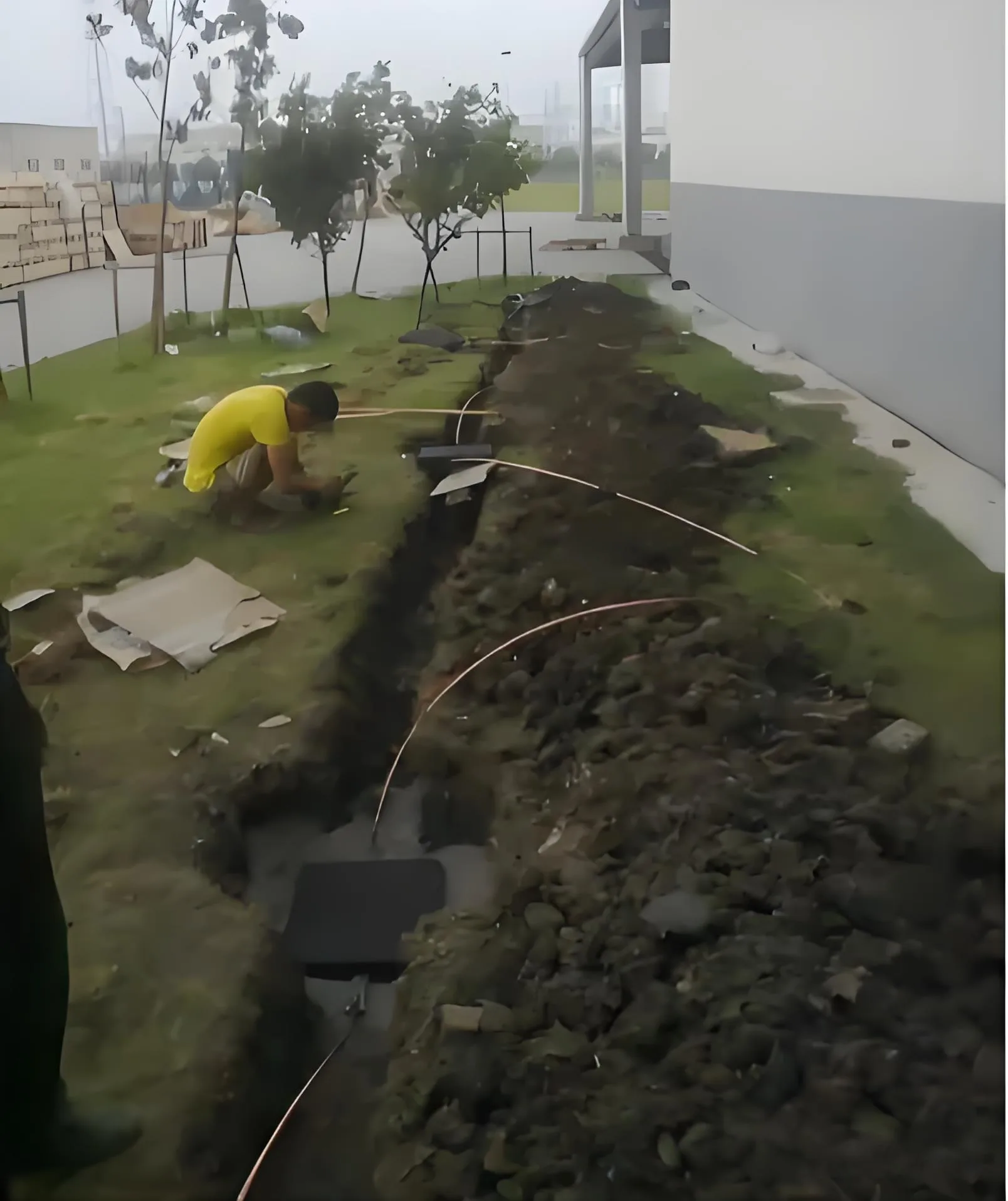

การติดตั้งต้องปฏิบัติตามขั้นตอนที่เข้มงวด: อิเล็กโทรดกราวด์ ESD (เช่น, 3แท่งหุ้มทองแดง ม. × φ20 มม) ถูกขับเคลื่อนในแนวตั้งจนถึงระดับความลึกอย่างน้อย 3 เมตรจากระดับพื้นผิว. มีอิเล็กโทรดอย่างน้อยสามอิเล็กโทรดจัดเรียงอยู่ในแนวเดียวกัน 3-5 ระยะห่างเมตร, ล้อมรอบด้วยวัสดุปรับปรุงดิน.

การทดสอบและการตรวจสอบความต้านทานกราวด์
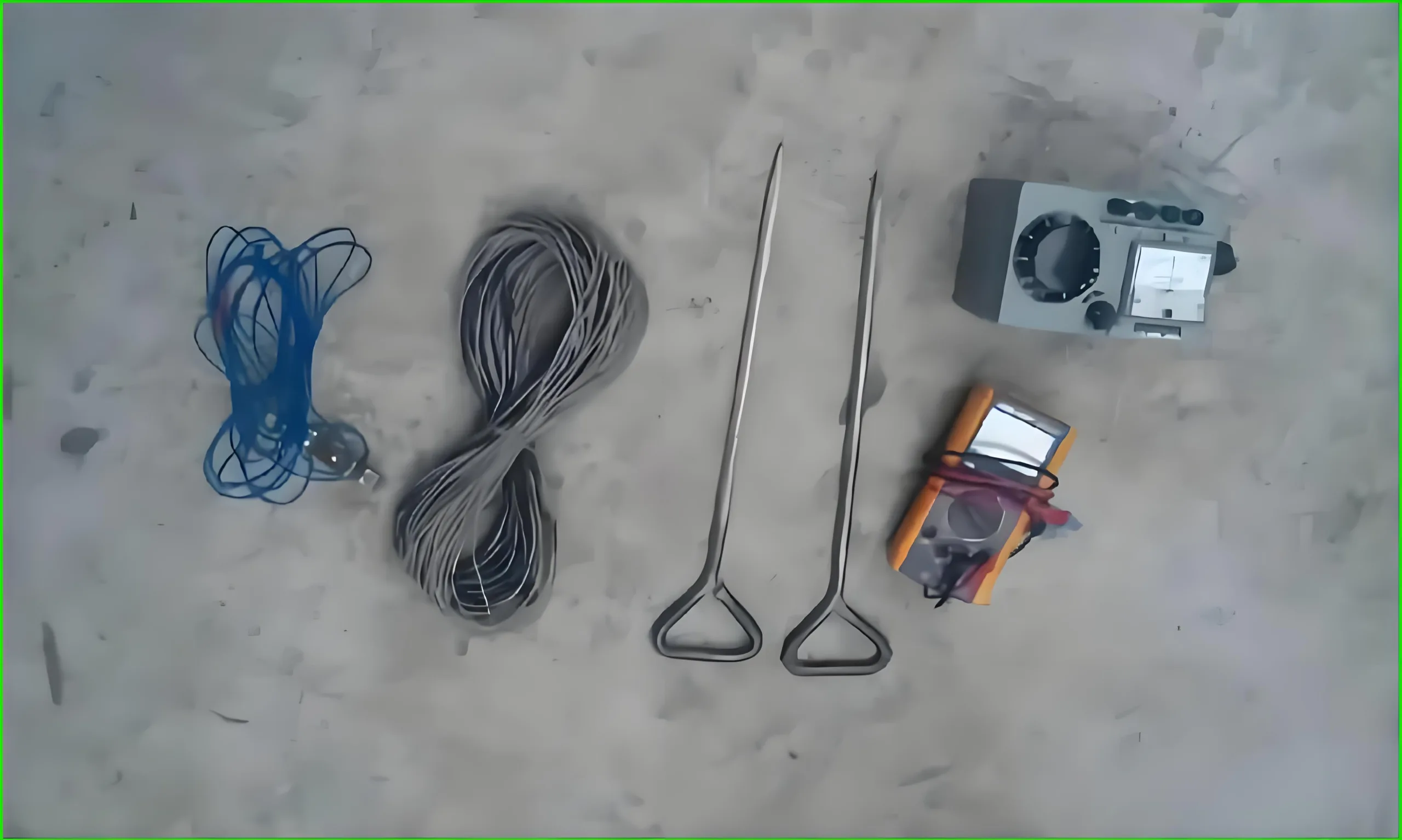
ประสิทธิภาพของระบบสายดินต้องได้รับการตรวจสอบผ่านการทดสอบเป็นระยะ. การใช้เครื่องทดสอบความต้านทานกราวด์, โดยการสอดโพรบทดสอบลงในดินเป็นอย่างน้อย 10 ห่างกันหลายเมตร, และวัดค่าความต้านทาน.
ควรทำการทดสอบอย่างน้อยปีละครั้งเพื่อให้มั่นใจถึงความน่าเชื่อถือของระบบ. ผลการทดสอบทั้งหมดจะต้องได้รับการบันทึกและวิเคราะห์แนวโน้มเพื่อระบุปัญหาที่อาจเกิดขึ้นในเชิงรุก.

แนวทางการจัดการ ESD และ MSD แบบบูรณาการ
ข้อกำหนดการควบคุมสิ่งแวดล้อม
การจัดการทั้ง ESD และ MSD ต้องการการควบคุมสิ่งแวดล้อมที่เข้มงวด. อุณหภูมิในพื้นที่ป้องกัน ESD (สำนักงานปกป้องสิ่งแวดล้อม) ควรรักษาอุณหภูมิไว้ที่ 23±3°C, โดยมีความชื้นสัมพัทธ์ระหว่าง 45-70%RH. การใช้งานอุปกรณ์ที่ไวต่อ ESD (SSD) ในสภาพแวดล้อมที่ต่ำกว่า 30%RH เป็นสิ่งต้องห้าม.
พื้นที่การผลิตจะต้องรักษาความสะอาด. ของใช้ส่วนตัวเช่นอาหาร, เครื่องดื่ม, กระเป๋า, ทำด้วยผ้าขนสัตว์, หนังสือพิมพ์, และห้ามใช้ถุงมือยางบนพื้นผิวงานของ EPA.
การฝึกอบรมบุคลากรและขั้นตอนการปฏิบัติงาน
บุคลากรทุกคนที่จัดการ MSD ต้องสวมถุงมือ ESD และสายรัดข้อมือ, ใช้มาตรการป้องกัน ESD เต็มรูปแบบ. ผู้ปฏิบัติงานจำเป็นต้องมีการฝึกอบรมด้านความปลอดภัยของ ESD และต้องผ่านการตรวจสอบที่เกี่ยวข้องก่อนจึงจะได้รับอนุญาตให้ผลิตได้.
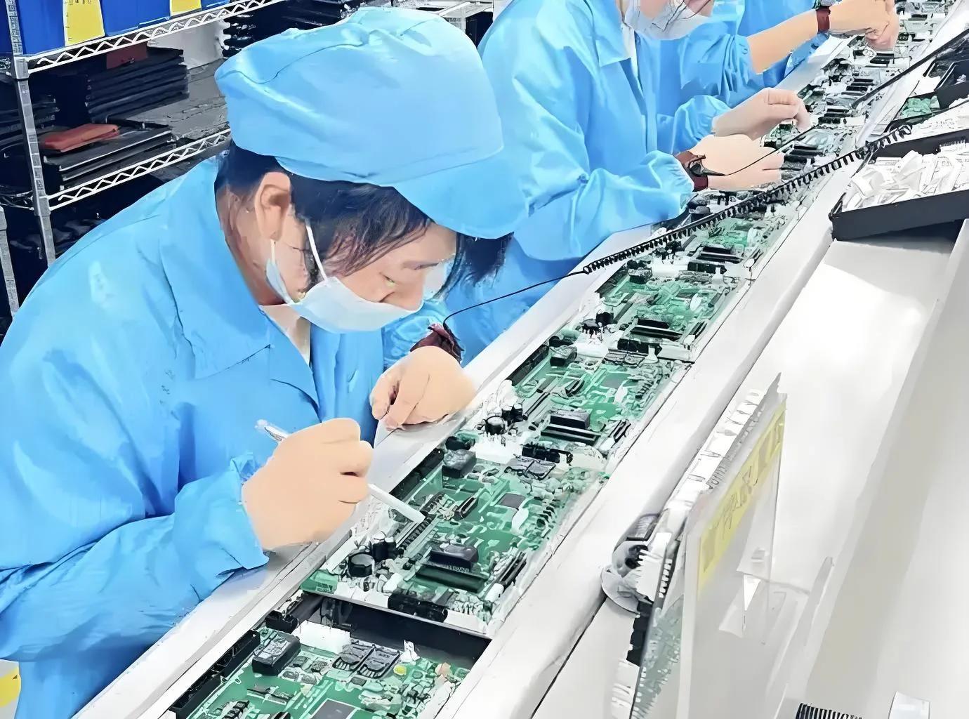

ผู้ปฏิบัติงานต้องสวมสายรัดข้อมือ ESD ที่ใช้งานได้, ตรวจสอบทุกวัน. สำหรับ MSD, ผู้ปฏิบัติงานจะต้องปฏิบัติตามกำหนดการผลิตอย่างเคร่งครัดเพื่อกำหนดปริมาณในการเปิด, หลีกเลี่ยงการสัมผัสโดยไม่จำเป็น.
การตรวจสอบและปรับปรุงอย่างต่อเนื่อง
การสร้างกลไกการตรวจสอบที่แข็งแกร่งเป็นกุญแจสำคัญในการรักษาการจัดการ ESD และ MSD ที่มีประสิทธิผลอย่างยั่งยืน. ไอพีคิวซี (การควบคุมคุณภาพในกระบวนการ) ต้องตรวจสอบการ์ดควบคุม MSD ในสายการผลิต, ตรวจสอบว่าเสร็จสมบูรณ์อย่างถูกต้องและตรงกับการปฏิบัติงานจริง, แก้ไขสิ่งที่ไม่เป็นไปตามข้อกำหนดโดยทันที.
วัดความต้านทานพื้นผิวของพื้นเป็นประจำ, พื้นผิวการทำงาน, และคอนเทนเนอร์เพื่อให้แน่ใจว่าการควบคุม ESD ทั้งหมดทำงานได้. สำหรับปัญหาที่ระบุ, ดำเนินการแก้ไขและติดตามประสิทธิผล.
บทสรุป: สร้างรากฐานสำหรับการผลิต PCB ที่เชื่อถือได้
การป้องกัน ESD และการจัดการ MSD ในการผลิต PCB ถือเป็นความท้าทายทางวิศวกรรมอย่างเป็นระบบ, ต้องการการควบคุมที่ครอบคลุมทั่วทั้งการออกแบบ, วัสดุ, กระบวนการ, สิ่งแวดล้อม, และบุคลากร. เมื่อเทคโนโลยีอิเล็กทรอนิกส์วิวัฒนาการ—ขับเคลื่อนด้วยความก้าวหน้าทางพลังงานใหม่, อาคารอัจฉริยะ, ไมโครกริดดีซี, ฯลฯ—ข้อกำหนดสำหรับการต่อสายดินของระบบและความปลอดภัยยังคงเพิ่มขึ้นอย่างต่อเนื่อง.
การสร้างระบบการจัดการทางวิทยาศาสตร์และการปฏิบัติตามมาตรฐานและข้อกำหนดที่เกี่ยวข้องอย่างเคร่งครัดเป็นวิธีเดียวที่จะเพิ่มความน่าเชื่อถือของ PCB/PCBA ได้อย่างมีประสิทธิภาพ, ปรับปรุงผลผลิตผ่านครั้งแรก, ลดความเสี่ยงด้านคุณภาพ, และรักษาความได้เปรียบในการแข่งขัน. สำหรับ ผู้ผลิต PCB, การใช้ระบบการจัดการ ESD และ MSD ที่แข็งแกร่งเพื่อเพิ่มความน่าเชื่อถือของผลิตภัณฑ์อย่างมีนัยสำคัญไม่ได้เป็นเพียงความจำเป็นในการตอบสนองความต้องการของลูกค้าเท่านั้น แต่ยังเป็นเส้นทางที่สำคัญในการเสริมสร้างความสามารถในการแข่งขันหลัก และวางรากฐานที่มั่นคงสำหรับการเติบโตของธุรกิจที่ยั่งยืน.