
อัน แผงวงจร ทินเนอร์กว่ากระดาษตอนนี้เป็นสนามรบที่สำคัญในการแข่งขันเทคโนโลยีระดับโลก. จากเซิร์ฟเวอร์ AI ไปจนถึงยานพาหนะอัจฉริยะ, ประสิทธิภาพของมันจะกำหนดความสำเร็จหรือความล้มเหลวของผลิตภัณฑ์อิเล็กทรอนิกส์โดยตรง.
ที่ห้องปฏิบัติการทดสอบของ UGPCB, วิศวกรวางเซิร์ฟเวอร์ AI ที่ผลิตใหม่ พีซีบี เข้าสู่สภาพแวดล้อมที่เย็นชา -55 ° C, จากนั้นโอนไปยังห้องอุณหภูมิสูง 125 ° C อย่างรวดเร็วหลังจากนั้น 30 ไม่กี่วินาที. การทดสอบวัฏจักรที่รุนแรงนี้ซ้ำ 1,000 เวลา-ทำให้มั่นใจได้ว่าวงจรไมครอนทุกระดับจะรักษาความเสถียรของสัญญาณภายใต้สภาวะที่รุนแรง.
“Our project nearly missed its deadline due to PCB signal interference!” lamented a tech company R&ผู้อำนวยการ D. ด้วย AI Computing Boom และ Smart Vehicle Architecture Revolution, การผลิต PCB ระดับสูงกำลังอยู่ระหว่างการเปลี่ยนแปลงทางเทคโนโลยีและการแข่งขันด้านกำลังการผลิตที่ไม่เคยมีมาก่อน.
01 การวิเคราะห์ห่วงโซ่อุตสาหกรรม: ระบบไหลเวียนโลหิตของการผลิต PCB
PCBS, hailed as the “Mother of Electronics,” form the core skeleton of nearly all electronic devices. เป็นแพลตฟอร์มพื้นฐานสำหรับส่วนประกอบ, พวกเขาเปิดใช้งานการเชื่อมต่อไฟฟ้าที่สำคัญ. คุณภาพของพวกเขาโดยตรงกำหนดความน่าเชื่อถือของผลิตภัณฑ์สุดท้าย, อายุขัย, และความสามารถในการแข่งขันของตลาด.
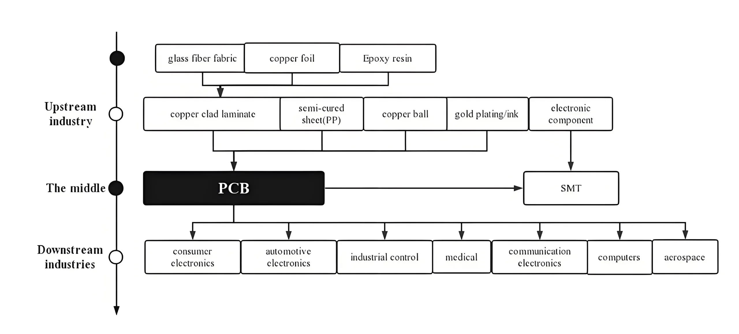

ต้นน้ำ: The “Three Kingdoms” Battle in Raw Materials
วัตถุดิบประกอบด้วย 60% ของค่าใช้จ่าย PCB, ด้วยแผ่นเคลือบทองแดงลามิเนต (CCL) บัญชีคนเดียวสำหรับ 27.31%. CCL เป็นวัสดุคอมโพสิตที่ประกอบด้วย:
-
ฟอยล์ทองแดง (42.1% ของค่าใช้จ่าย CCL): เซิร์ฟเวอร์ AI ผลักดันความต้องการที่เพิ่มขึ้นสำหรับฟอยล์ที่มีความรุนแรงต่ำ (ความบริสุทธิ์≥99.99%)
-
ผ้าไฟเบอร์กลาสอิเล็กทรอนิกส์ (ค่าใช้จ่าย ~ 27%): 5สถานีฐาน G & เซิร์ฟเวอร์ AI ต้องการผ้าแก้วต่ำ DK
-
เรซิ่นสังเคราะห์: ความต้องการเรซินที่ใช้น้ำเพิ่มขึ้น 15% YOY, ขับเคลื่อนโดย EU Rohs & มาตรฐานสิ่งแวดล้อมของจีน
กลางสตรีม: วิศวกรรมความแม่นยำในการผลิต PCB
PCB Manufacturing ผสมผสานศิลปะและวิศวกรรม. 8-Layer 3+N+3 บอร์ด HDI บรรลุ 2.5mil/2.5mil (≈0.063mm) ความกว้างของความกว้าง/ระยะห่าง, ด้วยความแม่นยำในการขุดเจาะด้วยเลเซอร์ภายใน±25μm.
การพัฒนากระบวนการที่สำคัญ:
-
การเพิ่มประสิทธิภาพแบบสแต็ก: ลดสัญญาณ crosstalk โดย 30% ผ่านการจำลองความต้านทาน
-
microvias ที่เซ: บรรลุ 15:1 อัตราส่วนภาพสำหรับการกำหนดเส้นทางที่มีความหนาแน่นสูง
-
24-การทดสอบอายุชั่วโมง: ตรวจสอบความน่าเชื่อถือภายใต้ความเครียด 85 ° C/85% RH
ข้อมูล prismark แสดง 2023-2028 การเจริญเติบโต: 18+ บอร์ดเลเยอร์ (9% cagr), China HDI (6% cagr, ผู้นำระดับโลก), พื้นผิว IC (7% cagr), PCB ที่ยืดหยุ่น (4% cagr).
ปลายน้ำ: การเติบโตอย่างระเบิดในแอปพลิเคชัน PCB
การคำนวณ AI และ Smart EV กำลังปรับเปลี่ยนความต้องการ PCB:
-
เซิร์ฟเวอร์ AI: ผลักดันปริมาณ/ราคา PCB ที่สูงขึ้น; เพิ่มความหนาแน่นของการคำนวณต่อชั้นวาง + การควบคุมความต้านทานอย่างเข้มงวดสำหรับ ชิป AI
-
ยานพาหนะพลังงานใหม่ (Nevs):
-
PCB Content 4-5X ยานพาหนะแบบดั้งเดิม
-
800แพลตฟอร์ม V ต้องการ 40% ความต้านทานแรงดันไฟฟ้าที่สูงขึ้น
-
เซ็นเซอร์ ADAS เพิ่มความต้องการ PCB ความถี่สูง
-
-
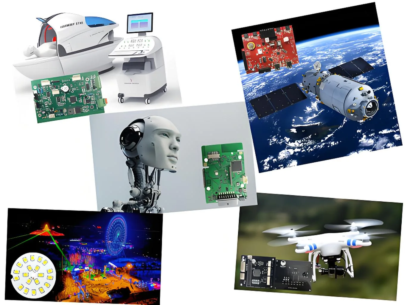
อุปกรณ์การแพทย์: อุปกรณ์ที่ฝังได้ต้องการการปนเปื้อนของไอออนิก≤1.56μg/cm² (NaCl Eq), เกินมาตรฐานผู้บริโภค.

02 การพัฒนาเทคโนโลยี: การต่อสู้ที่สำคัญสามครั้งในการผลิต PCB ขั้นสูง
การปฏิวัติวัสดุ PCB: จากฟิสิกส์พื้นฐานไปจนถึงผลกระทบควอนตัม
แอพพลิเคชั่นความถี่สูงต้องการวัสดุใหม่. 5สถานีฐาน G ต้องการการควบคุมอิมพีแดนซ์± 7% (>10กิกะเฮิรตซ์), Resin R Resin R&d:
สูตรวิทยาศาสตร์วัสดุ: Df = ε” / ε’
(ปัจจัยการกระจาย = การสูญเสียอิเล็กทริก / การอนุญาต)
วัสดุต่ำ DF/DK เป็นหัวใจสำคัญ. มาตรฐานอุตสาหกรรมเช่น PTFE ดัดแปลง (ฟ<0.001) และเรซินไฮโดรคาร์บอน (df = 0.001-0.002) ลดการสูญเสียสัญญาณ mmwave ด้วย 60%.
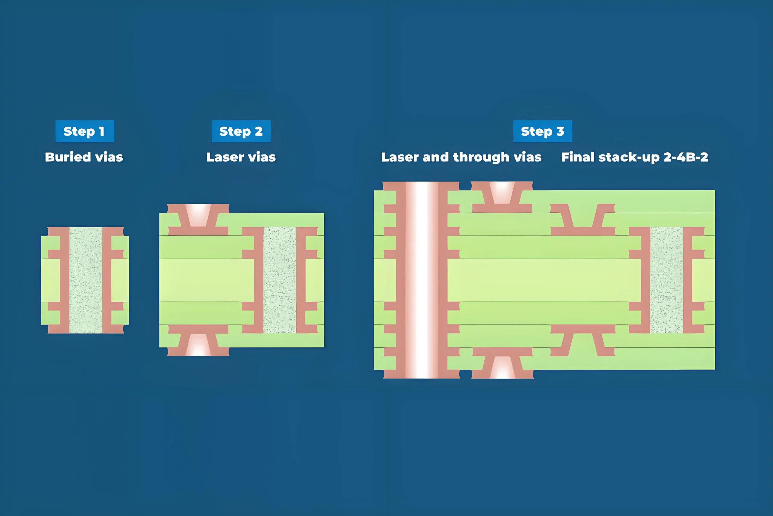
นวัตกรรมกระบวนการ PCB: ความท้าทายระดับไมครอน
ที่โรงงานอัจฉริยะของ UGPCB, การเจาะเลเซอร์กระบวนการ 8 ชั้น 3+N+3 HDI ที่ 300 หลุม/วินาที. ความก้าวหน้าที่สำคัญ:
-
การเชื่อมต่อระหว่างชั้นใด ๆ: เปิดใช้งาน 15:1 Microvias อัตราส่วนภาพ
-
การควบคุมความต้านทาน: ± 5% ความอดทน (VS. ± 7% สำหรับเรดาร์ยานยนต์)
-
เทคโนโลยีที่เข้มงวด: ยั่งยืน >100,000 โค้งงอ
การจัดตำแหน่งเลเยอร์ภายใน12μm (1/6 ผมของมนุษย์) ทำให้มั่นใจได้ว่า BGA เป็นโมฆะ <25% (คลาส IPC-A-610 3), ป้องกันความล้มเหลวในการบัดกรีชิป.

วิวัฒนาการการตรวจสอบ: ตั้งแต่หลังการผลิตจนถึงการทำนายแบบเรียลไทม์
การตรวจสอบเอ็กซ์เรย์อัตโนมัติที่เพิ่มขึ้น (แอ็กซี่) เพิ่มความเร็วในการตรวจสอบ BGA 5x, ลดการพลาด <0.1%. การวิเคราะห์ความล้มเหลวขั้นสูง:
-
การตรวจสอบภาพ (100กล้องจุลทรรศน์ x)
-
การทดสอบไฟฟ้า (เครื่องวิเคราะห์เครือข่าย)
-
X-ray/cross-section (SEM/EDS)
-
การถ่ายภาพความร้อน (การตรวจจับจุดร้อน)
PCBs เกรดยานยนต์ต้องการ -40 ° C ~ 125 ° C การปั่นจักรยานความร้อน (1,000 รอบ) กับ <0.01% ความต้านทานดริฟท์สำหรับแอปพลิเคชัน BMS.
03 การแข่งขันระดับโลก: การเปลี่ยนแปลงกำลังการผลิต & การวางตำแหน่งเทคโนโลยี
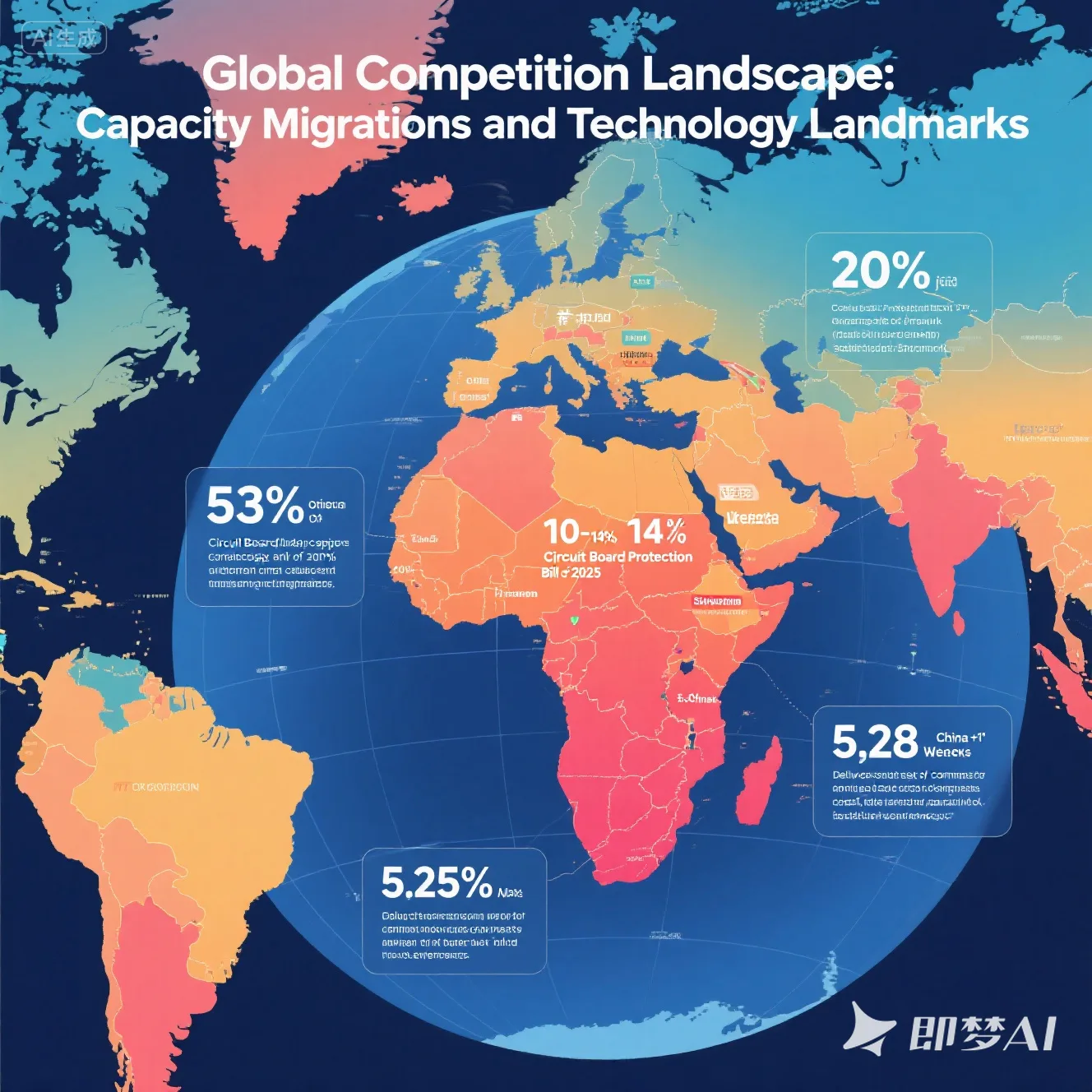
พลวัตระดับภูมิภาค: การปกครองของเอเชียแปซิฟิก
2025 ภูมิทัศน์ PCB: “East-led, multi-polar growth”:
-
จีน: 53% กำลังการผลิตระดับโลก (Prismark)
-
เอเชียตะวันออกเฉียงใต้: 20% การเจริญเติบโตของ YOY (ประเทศไทย, เวียดนาม)
-
สหรัฐอเมริกา: Subsidies via “Circuit Board Protection Act 2025”
การขึ้น PCB ระดับไฮเอนด์ของจีน
ในขณะที่จีนเป็นผู้นำในปริมาณ, เอาต์พุตของมันยังคงอยู่ระดับกลางถึงต่ำ (81% บอร์ดแข็ง). บริษัท ชั้นนำกำลังทำลายอุปสรรค:
-
วงจร Shennan: พื้นผิว FCBGA สำหรับ NVIDIA GPUS
-
UGPCB: PCBs เรดาร์ MMWave ที่ผ่านการรับรองจากยานยนต์ PCBS
-
Kinwong Electronics: การสื่อสารผ่านดาวเทียม SpaceX PCBS
Research Nester คาดการณ์ว่าตลาด PCB ทั่วโลกถึง $ 155.38B โดย 2037, ด้วยส่วนแบ่งระดับสูงของจีนอาจเพิ่มขึ้นจาก 15% ถึง 35%.
04 สนามรบในอนาคต: AI & การเจริญเติบโตของไดรฟ์ไฟฟ้า
คุณมีคอมพิวเตอร์: The “Dimensional Leap” for PCBs
การลงทุนโครงสร้างพื้นฐาน AI เปลี่ยนรูปแบบ PCB Tech:
-
บอร์ดเซิร์ฟเวอร์ AI: >20 ตอนนี้เลเยอร์ประกอบด้วย 60%
-
พื้นผิว HBM: ความกว้างของเส้น <8μm
-
โมดูลออปติคัล PCBS: 80% การยอมรับวัสดุที่สูญเสียไปต่ำ
AI Server PCB Market CAGR: 16% (น้ำค้างแข็ง & ซัลลิแวน). ใช้โทรศัพท์ AI 30% เลเยอร์มากขึ้นและ 15 FPCS/หน่วย, เร่งการยอมรับ HDI.

การปฏิวัติ EV: Reengineering the Automotive “Heart”
NEV Electronics สร้างมาตรฐาน PCB ยานยนต์ใหม่:
-
ตัวควบคุมโดเมน: 8-12 เลเยอร์ HDI Dominance
-
บอร์ด LiDAR: วัสดุ PTFE ความถี่สูง
-
800แพลตฟอร์ม V: ฉนวนกันความร้อนทน≥3kV
2025 ยอดขาย NEV: ~ 15m หน่วย. ค่า PCB/ยานพาหนะ 4x Ice Cars. BMS PCB ต้องการ 0.01% เสถียรภาพความต้านทาน (-40° C ~ 125 ° C).
การผลิตที่ยั่งยืน: ความจำเป็นในการปฏิบัติตามกฎระเบียบ
กฎระเบียบข้อบังคับของสหภาพยุโรป EPR:
-
100% ประสานกันตะกั่วโดย 2026
-
95% อัตราการรีไซเคิลทองแดง
-
≥30% เรซินที่ใช้ชีวภาพ
ความต้องการมาตรฐานการปล่อยมลพิษของจีน 40% การลด VOC, การผลักดันการใช้หมึกที่ใช้น้ำในการพิมพ์ PCB จาก 35% ถึง 65% โดย 2027.
05 บทสรุป: การวางตำแหน่งเชิงกลยุทธ์ & ทางเลือก
อุตสาหกรรม PCB ทั่วโลกกำลังอยู่ระหว่างการเปลี่ยนแปลงอย่างลึกซึ้ง. Mordor Intelligence คาดการณ์การเติบโตของตลาดจาก $ 84.24B (2025) ถึง $ 106.85B (2030) ที่ 4.87% cagr. โอกาสสำคัญ:
-
กำลังการผลิตระดับสูง: 18+ บอร์ดเลเยอร์ (9% cagr), การขาดแคลนสารตั้งต้น IC (30%)
-
การเปลี่ยนแปลงระดับภูมิภาค: 25% ลดต้นทุนการตั้งค่าในเอเชียตะวันออกเฉียงใต้
-
นวัตกรรมวัสดุ: วัสดุ DK/DF ต่ำ (40% การเติบโตของความต้องการของ YOY)

บันทึก: ข้อมูลที่นำเสนอในเอกสารนี้มาจากรายงานล่าสุดของสถาบันที่มีสิทธิ์รวมถึง Prismark, IPC, และน้ำค้างแข็ง & ซัลลิแวน. พารามิเตอร์ทางเทคนิคทั้งหมดได้รับการตรวจสอบผ่านการทดสอบอย่างเข้มงวดที่ดำเนินการในห้องปฏิบัติการที่ได้รับการรับรอง CNAS. มาตรฐานกระบวนการปฏิบัติตามข้อกำหนดของรุ่นปัจจุบันเช่น IPC-6012EM* และ IPC-2221B.