
What is a 12L 2+N+2 HDI PCB?
A 12L 2+N+2 HDI PCB refers to a twelve-layer การเชื่อมต่อระหว่างกันที่มีความหนาแน่นสูง (HDI) แผงวงจรพิมพ์, featuring two core layers flanked by N signal layers and another two core layers. This configuration allows for high density interconnections, making it suitable for advanced electronic applications. The “2+N+2” designation indicates the arrangement of the core and signal layers.

ข้อควรพิจารณาในการออกแบบ
Designing a 12L 2+N+2 HDI PCB involves several critical factors:
- การซ้อนชั้น: Proper alignment of the core and signal layers to ensure optimal electrical performance.
- ติดตามและพื้นที่: Minimal trace width and space of 3mil/3mil to accommodate fine features.
- Hole Sizes: Mechanical holes as small as 0.2mm and laser holes down to 0.1mm for precise component placement.
- ความหนาของทองแดง: Varied copper thickness with inner layers at 1OZ and outer layers at 0.5OZ to balance conductivity and flexibility.
มันทำงานอย่างไร?
The functionality of a 12L 2+N+2 เอชดีไอ พีซีบี relies on its multilayer structure and the use of high-density interconnects. Each layer serves a specific purpose:
- Core Layers: Provide structural integrity and act as the foundation for signal layers.
- Signal Layers: Carry electrical signals between components.
- การรักษาพื้นผิว: Immersion gold plus OSP ensures excellent solderability and long-term reliability by preventing oxidation.
การใช้งานและการจำแนกประเภท


วัสดุและประสิทธิภาพ
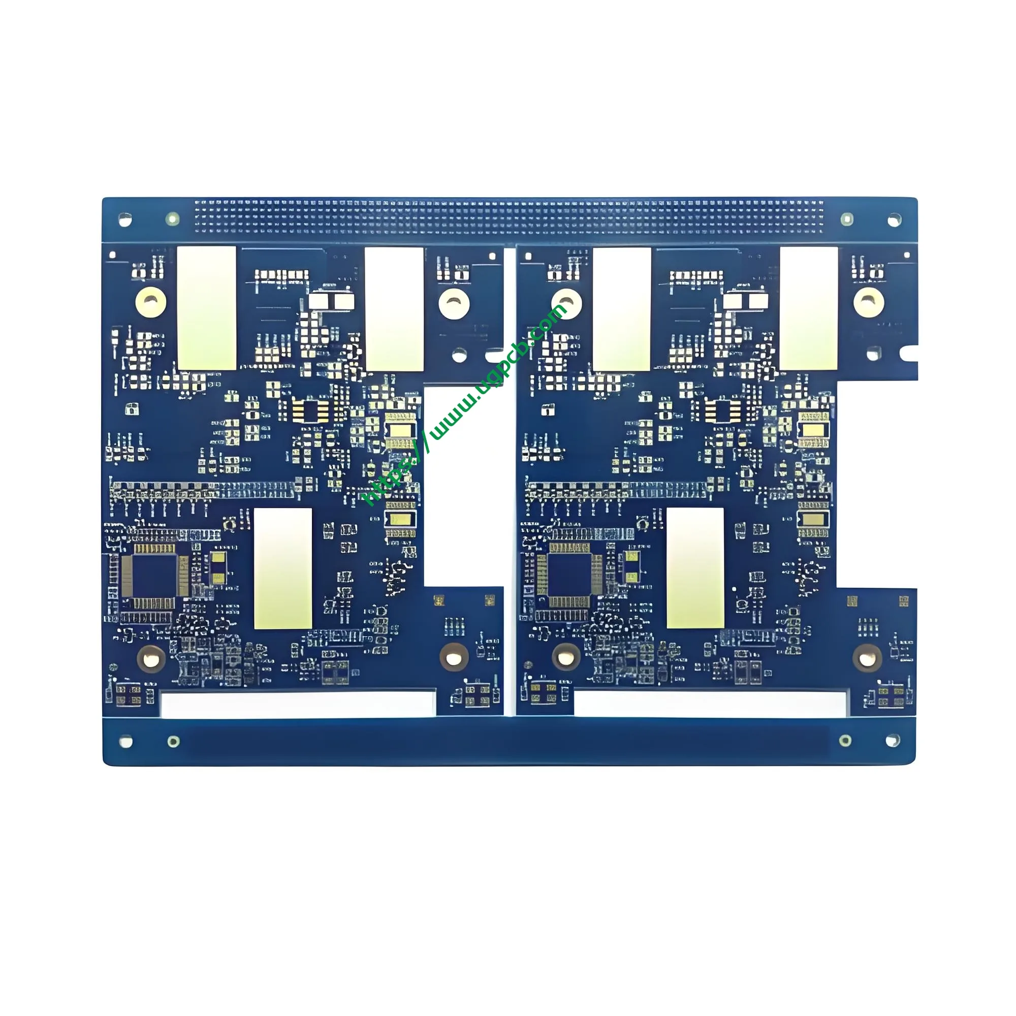
Constructed from FR-4 ITEQ, these PCBs offer excellent thermal stability and mechanical strength. The blue/white color scheme aids in visual inspection and troubleshooting. The finished thickness of 1.6mm provides a robust yet flexible board suitable for intricate designs.
โครงสร้างและคุณลักษณะ
The unique structure of a 12L 2+N+2 HDI PCB includes:
- Twelve Layers: Two core layers, N signal layers, and another two core layers.
- High Density Interconnects: Allow for complex routing and minimal space usage.
- การรักษาพื้นผิว: Immersion gold plus OSP enhances conductivity and protects against corrosion.
กระบวนการผลิต
The manufacturing process involves several sophisticated steps:
- การเตรียมวัสดุ: Selecting high-quality FR-4 substrate and copper foils.
- การซ้อนชั้น: Arranging the layers in a precise order to achieve the desired “2+N+2” configuration.
- พันธะ: การใช้ความร้อนและแรงกดเพื่อยึดชั้นต่างๆ เข้าด้วยกัน.
- การแกะสลัก: ใช้ etchant เพื่อขจัดทองแดงส่วนเกิน, เหลือเพียงเส้นทางนำไฟฟ้าที่ต้องการ.
- การชุบ: Adding a thin layer of metal to improve conductivity and solderability.
- การรักษาพื้นผิว: Applying immersion gold plus OSP to protect against oxidation and enhance solderability.
- การควบคุมคุณภาพ: ดำเนินการตรวจสอบและทดสอบอย่างละเอียดเพื่อให้แน่ใจว่าบอร์ดแต่ละบอร์ดมีคุณสมบัติตรงตามมาตรฐานคุณภาพที่เข้มงวด.


กรณีการใช้งานและสถานการณ์
12L 2+N+2 HDI PCBs are ideal for use in intelligent digital products where miniaturization and high performance are critical. แอปพลิเคชันทั่วไปรวมถึง:
- สมาร์ทโฟน: ช่วยให้มีการออกแบบที่เพรียวบางขึ้นโดยไม่กระทบต่อฟังก์ชันการทำงานหรือประสิทธิภาพ.
- เม็ด: ให้การเชื่อมต่อที่เชื่อถือได้สำหรับการถ่ายโอนและประมวลผลข้อมูลความเร็วสูง.
- อุปกรณ์สวมใส่ได้: รองรับการออกแบบที่กะทัดรัดในขณะที่ยังคงประสิทธิภาพและความทนทานที่แข็งแกร่ง.
- เครื่องเล่นมีเดียแบบพกพา: รับประกันความสามารถในการประมวลผลเสียงและวิดีโอคุณภาพสูงในรูปแบบขนาดเล็ก.
สรุปแล้ว, the 12L 2+N+2 HDI PCB represents a pinnacle of innovation in PCB technology, ให้ความหนาแน่นที่ไม่มีใครเทียบได้, ผลงาน, และความน่าเชื่อถือสำหรับแอปพลิเคชันอิเล็กทรอนิกส์สำหรับผู้บริโภคที่มีความต้องการมากที่สุด.