

UGPCB ห้องปฏิบัติการเคมี: เครื่องยนต์เทคโนโลยีหลักในการผลิต PCB
การแนะนำ
ในอุตสาหกรรมการผลิตอุปกรณ์อิเล็กทรอนิกส์, แผงวงจรพิมพ์ (PCBS) ทำหน้าที่เป็นผู้ขนส่งพื้นฐานของผลิตภัณฑ์อิเล็กทรอนิกส์, ซึ่งคุณภาพส่งผลโดยตรงต่อประสิทธิภาพและความน่าเชื่อถือของผลิตภัณฑ์ขั้นสุดท้าย. ในฐานะผู้นำด้านการให้บริการ PCB, พีซีบี, และ พีอีซีวีดี บริการ, UGPCB ดำเนินกิจการห้องปฏิบัติการเคมีที่ทำหน้าที่หลัก เช่น การวิเคราะห์วัสดุ, การเพิ่มประสิทธิภาพกระบวนการ, และการควบคุมคุณภาพ. บทความนี้ให้การวิเคราะห์เชิงลึกเกี่ยวกับระบบปฏิบัติการของห้องปฏิบัติการ และเน้นย้ำถึงบทบาทที่สำคัญในการผลิต PCB.
แผนผังห้องปฏิบัติการและระบบอุปกรณ์
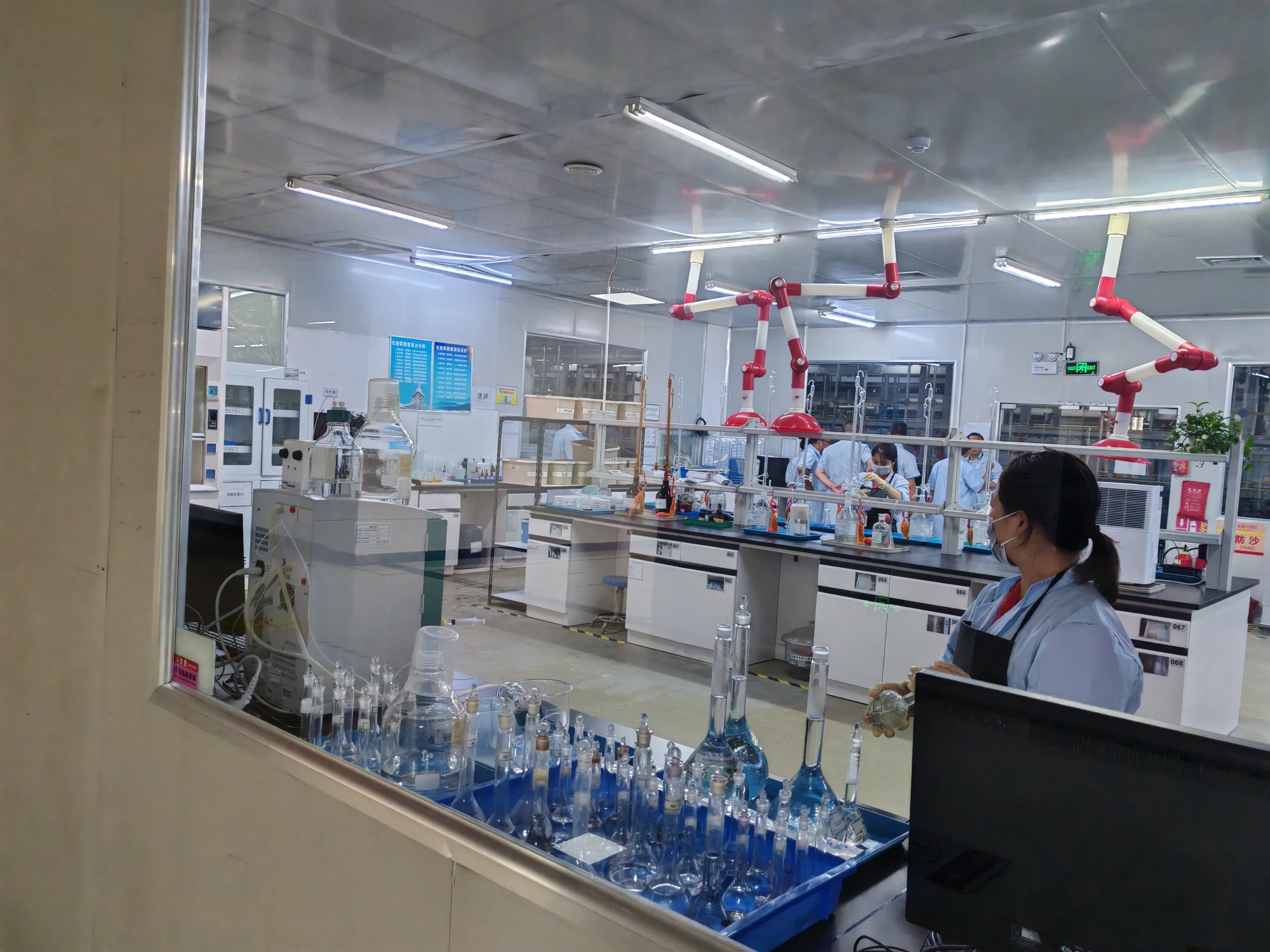
โซนทดลองกลาง
ที่ UGPCB ห้องปฏิบัติการใช้การออกแบบโมดูลาร์โดยมีพื้นที่หลักดังต่อไปนี้:
โซนทดลองกลาง
-
ติดตั้งโต๊ะทำงานที่ทนต่อการกัดกร่อนที่เคลือบด้วยเรซิน EPOXY เพื่อทนทานต่อกรดและด่างแก่. เครื่องแก้ว เช่น บีกเกอร์ และกระบอกตวง ได้รับการจัดเรียงอย่างประณีต, และขวดรีเอเจนต์จะจัดเก็บไว้ในถาดสีน้ำเงินตามประเภท, การนำการจัดการ 5ส ไปใช้.
ระบบระบายอากาศ
-
ท่อไอเสียสีแดงเชื่อมต่อกับตู้ดูดควันหลายตัวช่วยให้มั่นใจได้ถึงความเร็วการไหลของอากาศ 0.5 เมตร/วินาที, เก็บไอตัวทำละลายอินทรีย์ (เช่น, อะซิโตน, ไอโซโพรพิลแอลกอฮอล์) ความเข้มข้นต่ำกว่าขีดจำกัดการรับสัมผัสในการทำงาน.
โซนตรวจสอบความแม่นยำ
-
กำหนดค่าด้วยเครื่องสเปกโตรโฟโตมิเตอร์ (สำหรับการตรวจจับความเข้มข้นของไอออนทองแดง), สเปกโตรมิเตอร์การดูดซึมอะตอม (สำหรับการวิเคราะห์สารตกค้างของโลหะหนัก), และเครื่องวัดความหนาผิวเคลือบ XRF (ความแม่นยำ ±0.1 ไมโครเมตร). ระยะห่างของอุปกรณ์เป็นไปตามมาตรฐาน ISO 14644-1 มาตรฐานห้องสะอาด.
การวิเคราะห์กระบวนการ PCB หลัก
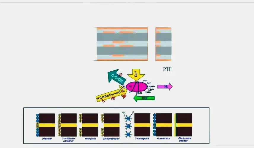
กระบวนการชุบทองแดงแบบไม่ใช้ไฟฟ้า PCB
กระบวนการนี้เป็นไปตามกลไกปฏิกิริยาสามขั้นตอน:
การปรับสภาพ (ระบบอัลคาไลน์โพแทสเซียมเปอร์แมงกาเนต)
MnO₄⁻ + H₂O → MnO₂ + 2โอ้⁻ + O₂↑
การทำความสะอาดอัลตราโซนิกจะขจัดคราบเรซินออกจาก พีซีบี ผนังหลุม, โดยควบคุมความหยาบไว้ที่ Ra 0.15–0.3 μm.
การเปิดใช้งาน (ระบบคอลลอยด์แพลเลเดียม)
PD²⁺ + Sn²⁺ → Pd-Sn อนุภาคคอลลอยด์
ความช่วยเหลืออัลตราโซนิกช่วยให้มั่นใจได้ว่าการดูดซับตัวเร่งปฏิกิริยาสม่ำเสมอบนไมโครเวีย (≥0.15 มม) ผนังด้านใน.
การสะสมของทองแดง (ระบบลดฟอร์มาลดีไฮด์)
คิว²⁺ + ฮชอ + OH⁻ → Cu↓ + HCOO⁻ + เอช₂โอ
พารามิเตอร์ที่สำคัญ: ค่า pH 9.0–9.5, อุณหภูมิ 30±0.5°C, อัตราการสะสม 2 ไมโครเมตร/15 นาที, ความหนาของทองแดง ≥1.5 μm (ตามมาตรฐาน IPC-6012).

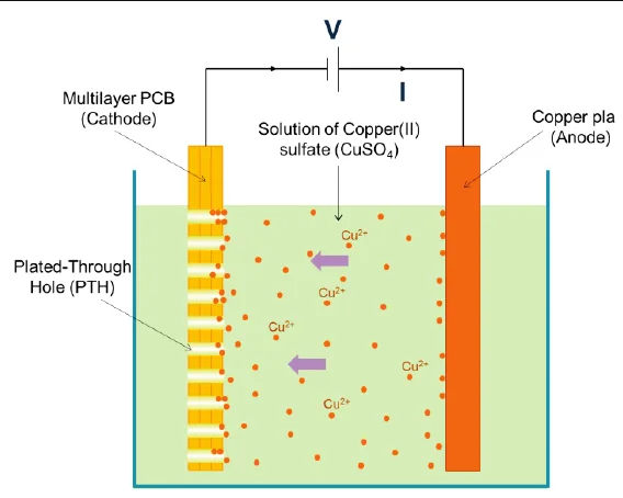
การเพิ่มประสิทธิภาพกระบวนการชุบด้วยไฟฟ้า PCB
การใช้ Hull Cell เพื่อจำลองสภาวะการผลิต, ปฏิกิริยาต่อไปนี้ช่วยให้มั่นใจได้ถึงความสม่ำเสมอของการชุบ:
ขั้วบวก: ลูกบาศ์ก → Cu²⁺ + 2อี⁻
แคโทด: คิว²⁺ + 2อี⁻ → Cu↓
พารามิเตอร์ที่สำคัญ: ความหนาแน่นกระแส 1.5 A/dm², อุณหภูมิอ่าง 25±1°C, ความเข้มข้นของสารเติมแต่งคงอยู่ที่ PCA 5–8 มล./ลิตร, รับประกันความเบี่ยงเบนของความหนาของทองแดงบนผนังรู ≤5%.

ระบบความปลอดภัยและการควบคุมคุณภาพ
โปรโตคอลความปลอดภัยในห้องปฏิบัติการ
-
มาตรการป้องกัน: ผู้ปฏิบัติงานสวมถุงมือไนไตรล์, แว่นตา, และผ้ากันเปื้อนป้องกันไฟฟ้าสถิต; มีการเพิ่มแผ่นป้องกันใบหน้าเมื่อต้องจัดการกับกรดแก่.
-
การบำบัดของเหลวเสีย: ของเสียที่มีทองแดงจะถูกรีไซเคิลผ่านเรซินแลกเปลี่ยนไอออนด้วย >60% อัตราการฟื้นตัว; ขยะอินทรีย์จะได้รับการบำบัดด้วยการดูดซับถ่านกัมมันต์ก่อนเข้าสู่ ระบบเตาเผา RTO.
-
การจัดการเหตุฉุกเฉิน: มีจุดล้างตาฉุกเฉินและที่อาบน้ำ; เวลาตอบสนองจากสถานีดับเพลิงที่ใกล้ที่สุดคือ ≤3 นาที.
ระบบตรวจสอบแบบเรียลไทม์
-
การวิเคราะห์ออนไลน์: เครื่องวัดค่าการนำไฟฟ้าจะตรวจสอบสิ่งเจือปนในอ่างชุบ; การเติมน้ำบริสุทธิ์อัตโนมัติจะทำงานเมื่อความเข้มข้นของ Cl⁻ เกิน 50 PPM.
-
การจัดการตรวจสอบย้อนกลับ: บันทึกแบทช์แต่ละรายการจะมีหมายเลขล็อตของรีเอเจนต์, วันที่สอบเทียบอุปกรณ์, และลายเซ็นผู้ดำเนินการ, สอดคล้องกับมาตรฐาน ISO 17025 ข้อกำหนดการรับรองห้องปฏิบัติการ.
การประยุกต์ทางอุตสาหกรรมและนวัตกรรมทางเทคโนโลยี
การเปรียบเทียบกระบวนการบำบัดพื้นผิว PCB
| ประเภทกระบวนการ | สถานการณ์การใช้งาน | พารามิเตอร์ที่สำคัญ |
|---|---|---|
| เห็นด้วย | การเชื่อมต่อระหว่างกันที่มีความหนาแน่นสูง (บีจีเอ/ซีเอสพี) | ความหนาของนิกเกิล 3–5 μm, ความหนาของทองคำ 0.05–0.1 μm |
| โอป | อุปกรณ์อิเล็กทรอนิกส์สำหรับผู้บริโภค (มือถือ/แท็บเล็ต) | ความหนาของฟิล์ม 0.2–0.5 μm, อายุการเก็บรักษา ≤6 เดือน |
| กระป๋อง | อุปกรณ์อิเล็กทรอนิกส์ยานยนต์ (ทนต่ออุณหภูมิสูง) | ความหนาของดีบุก 1.0±0.2 μm, อัตรามัสสุ <2% |
กรณีศึกษาที่ก้าวหน้า
สำหรับโครงการบอร์ดสื่อสาร 5G, UGPCB ใช้ระบบการชดเชยพารามิเตอร์แบบไดนามิก, การบรรลุเป้าหมาย:
-
30% การปรับปรุงความสม่ำเสมอของความหนาของทองแดง microvia (ซีพีเค >1.33)
-
ยืดอายุสารละลายทองแดงแบบไม่ใช้ไฟฟ้าให้ยาวนานขึ้น 120 ตร.ม./ลิตร (ค่าเฉลี่ยอุตสาหกรรม: 80 ตร.ม./ลิตร)
-
100% อัตราการผ่านในการทดสอบการเปลี่ยนแปลงอุณหภูมิอย่างฉับพลัน (288°ซ × 10 วินาที × 3 รอบ)
บทสรุป
ห้องปฏิบัติการเคมี UGPCB รับประกันคุณภาพตั้งแต่ต้นทางถึงปลายทาง—ตั้งแต่การวิเคราะห์วัสดุไปจนถึงการตรวจสอบยืนยันผลิตภัณฑ์ขั้นสุดท้าย—ผ่านการควบคุมกระบวนการที่แม่นยำ, การจัดการความปลอดภัยที่เข้มงวด, และนวัตกรรมทางเทคโนโลยีอย่างต่อเนื่อง. พารามิเตอร์ทางเทคนิคหลักเป็นไปตามมาตรฐานสากล เช่น IPC-4552A และ JPCA-ET01, ให้การสนับสนุนที่เชื่อถือได้สำหรับแอปพลิเคชันระดับไฮเอนด์ รวมถึงสถานีฐาน 5G, อุปกรณ์อิเล็กทรอนิกส์ยานยนต์, และอุปกรณ์การแพทย์, แสดงให้เห็นถึงความสามารถขั้นสูงของการผลิต PCB ของจีน.