
مقدمة
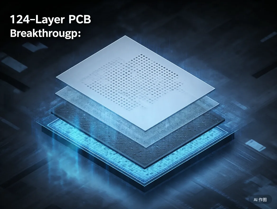
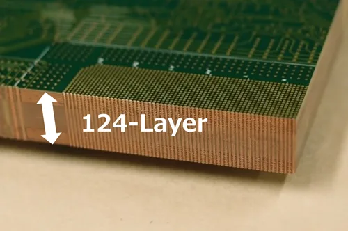
Driven by artificial intelligence (منظمة العفو الدولية) and high-performance computing (HPC), the global electronics industry is undergoing a technological revolution centered on “high density, سرعة عالية, and high reliability.” In May 2025, a leading الشركة المصنعة لثنائي الفينيل متعدد الكلور unveiled the world’s first commercial 124-layer printed circuit board, breaking the longstanding 108-layer industry barrier while maintaining the standard 7.6mm board thickness. This milestone not only provides critical hardware support for AI servers, semiconductor testing, and defense systems but also unlocks new frontiers in electronic packaging technology.
Breaking the 108-Layer Barrier: Engineering Solutions Behind 124-Layer PCBs
Precision Manufacturing Innovations
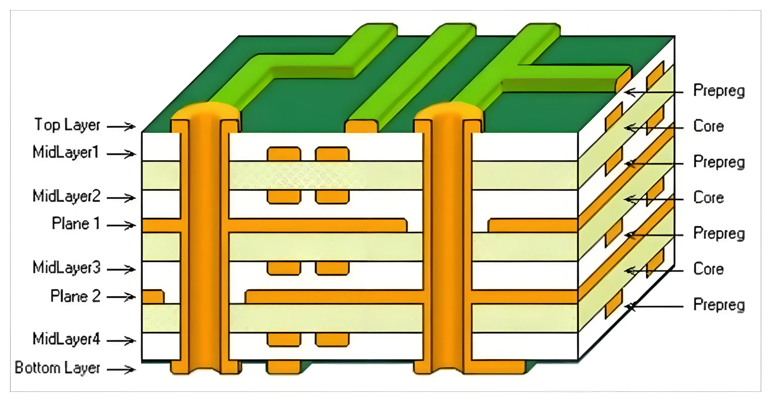
تقليدي PCB designs face mechanical and thermal limitations at 100 layers due to resin flow inconsistencies, via collapse, and layer misalignment. The breakthrough 124-layer PCB achieves a 15% layer increase through:
-
Ultra-Thin Dielectrics: 25µm layers using low-loss materials (على سبيل المثال, ميجاترون 7) with ±5% impedance control for 112+ GHz signals
-
3D Interconnect Optimization: Microvia arrays enabling 0.15mm²/mm signal density, compliant with PCIe Gen6 and CXL 3.0 protocols
Thermal Reliability Certification
Certified under MIL-STD-883G standards, the 124-layer PCB withstands 1,000+ الدورات الحرارية (-55°C to 125°C) while maintaining <1% signal loss at 80 MPa mechanical stress – making it ideal for aerospace and defense applications.
التطبيقات: Accelerating AI Hardware and Semiconductor Advancements
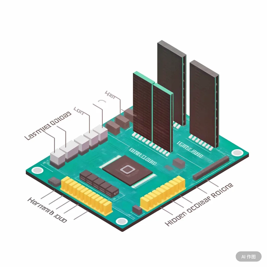
AI Servers & High-Bandwidth Memory (HBM)
-
Signal Density: 18% increase in differential pair routing per layer
-
الإدارة الحرارية: Copper-filled microvias improve thermal conductivity by 30%, critical for 500W+ AI accelerators
اختبار على مستوى الويفر & 3D Packaging
Enables sub-micron alignment accuracy (±0.8µm) and picosecond-level signal delay control for stacked HBM modules – a game-changer for chiplet-based architectures.
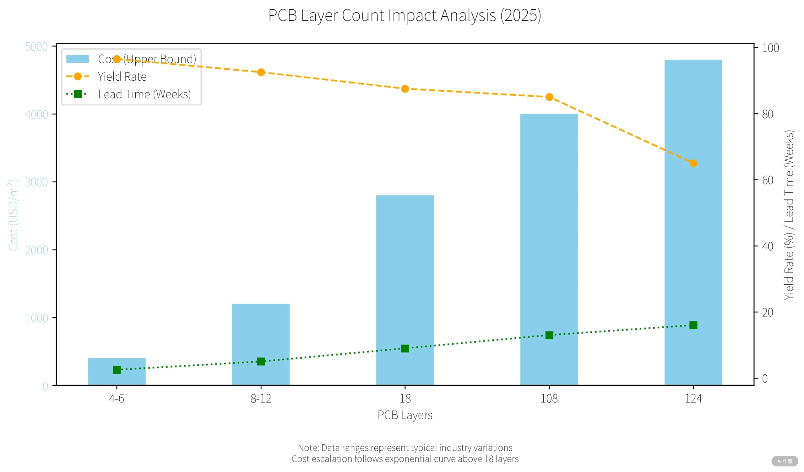
Cost Challenges & Scalability Roadmap
Manufacturing Economics
-
Material Cost: 4,800/m2(vs.3,200/m² for 108-layer)
-
Yield Rates: 65% (16-week cycle) vs. 85% for conventional مؤشر التنمية البشرية
-
Failure Analysis: Destructive cross-sectioning required for 20% of thermal stress defects
Industrial Adoption Pathways
-
Additive Manufacturing: Reduces lamination steps by 40%
-
AI-Driven EDA: Predicts via stress points with 92% accuracy, potentially boosting yields to 75%
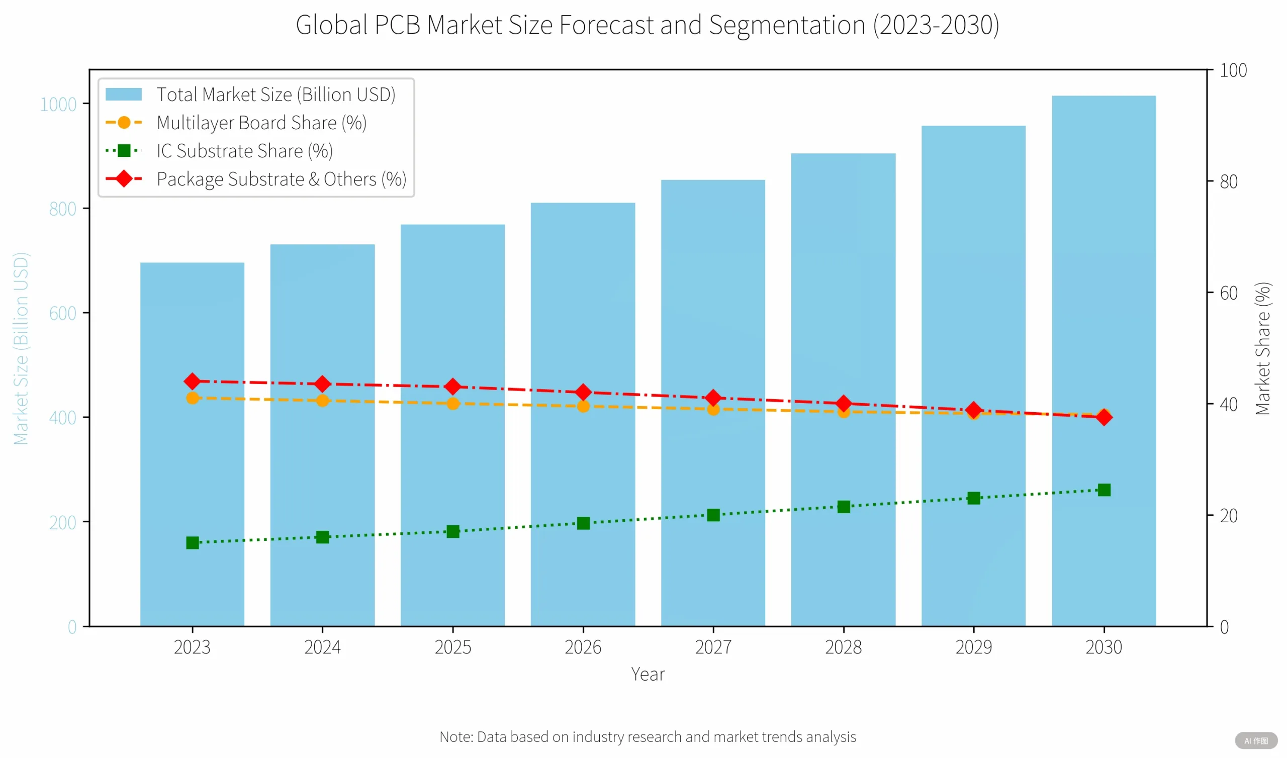
Market Outlook: $49B PCB Industry Transformation
Growth Drivers
-
Cloud Computing: 70% CAGR in AI server PCBs (Citic Securities 2026 projection)
-
Edge AI Devices: 30% PCB cost increase in next-gen smartphones (Apple’s Supply Chain Data)
-
Localization Trends: Chinese manufacturers like UGPCB targeting 3.6M m²/year capacity for advanced substrates
خاتمة: Practical Innovation Over Layer Count Records
While not surpassing Denso’s 129-layer prototype (2012), this 124-layer PCB sets a new commercial benchmark through:
-
Standardized thickness (7.6مم) for backward compatibility
-
MIL-SPEC reliability at 85% of prototype costs
-
Scalable manufacturing processes
As quantum computing and 6G emerge, PCB innovation will prioritize functional density over layer count – a crucial shift for sustainable technological progress.
