
أ لوحة الدائرة thinner than paper is now a critical battlefield in global tech competition. From AI servers to smart vehicles, its performance directly determines the success or failure of electronic products.
At UGPCB’s testing lab, engineers place a newly produced AI server ثنائي الفينيل متعدد الكلور into a -55°C extreme cold environment, then rapidly transfer it to a 125°C high-temperature chamber after 30 ثواني. This harsh cycle test repeats 1,000 times – ensuring every micron-level circuit maintains signal stability under extreme conditions.
“Our project nearly missed its deadline due to PCB signal interference!” lamented a tech company R&D director. With the AI computing boom and smart vehicle electronic architecture revolution, high-end PCB manufacturing is undergoing unprecedented technological transformation and capacity competition.
01 Industry Chain Analysis: The Circulatory System of PCB Manufacturing
مركبات ثنائي الفينيل متعدد الكلور, hailed as the “Mother of Electronics,” form the core skeleton of nearly all electronic devices. As the foundational platform for components, they enable critical electrical connectivity. Their quality directly determines end-product reliability, lifespan, and market competitiveness.
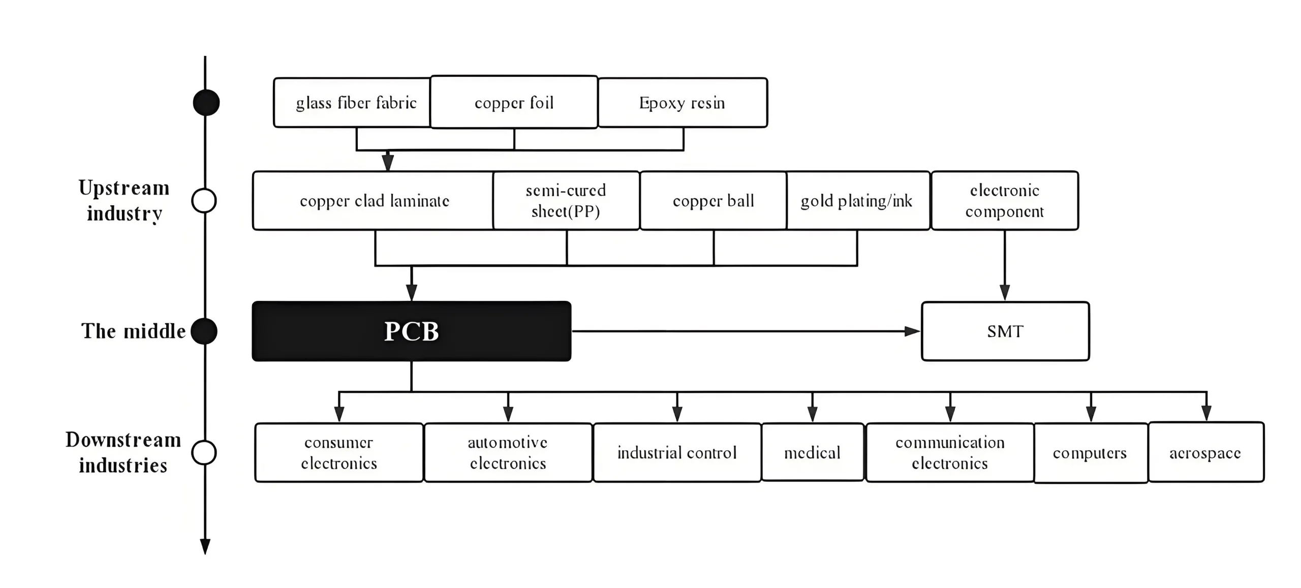
Upstream: ال “Three Kingdoms” Battle in Raw Materials
Raw materials constitute 60% of PCB costs, with Copper Clad Laminate (سي سي إل) alone accounting for 27.31%. CCL is a composite material comprising:
-
احباط النحاس (42.1% of CCL cost): AI servers drive surging demand for low-roughness foil (purity ≥99.99%)
-
Electronic Fiberglass Fabric (~27% cost): 5G base stations & AI servers require low-Dk glass fabric
-
Synthetic Resin: Water-based resin demand grows 15% YoY, driven by EU RoHS & China’s eco-standards
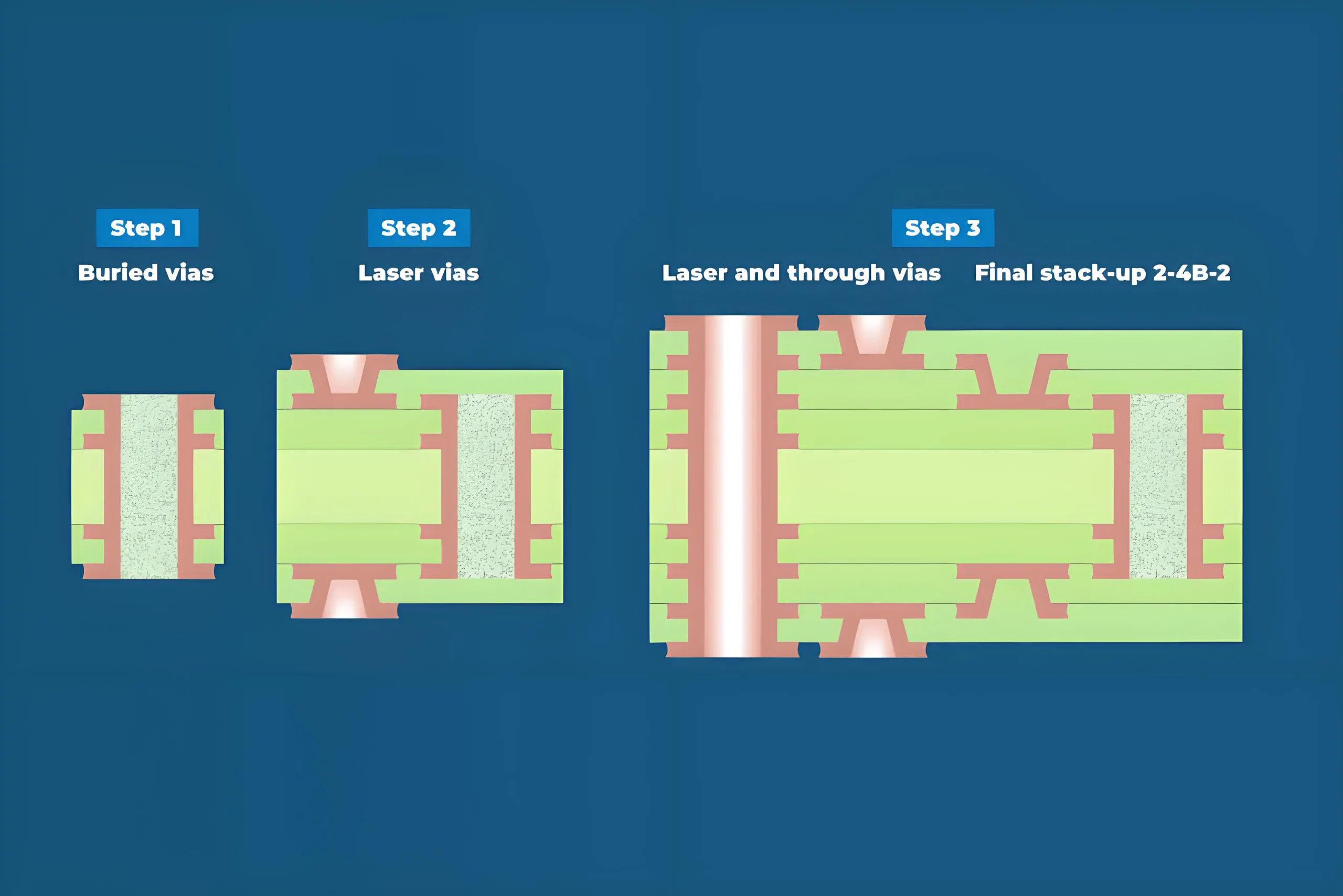
Midstream: Precision Engineering in PCB Fabrication
PCB manufacturing blends art and engineering. Cutting-edge 8-layer 3+N+3 HDI boards achieve 2.5mil/2.5mil (≈0.063mm) line width/spacing precision, with laser drilling accuracy within ±25μm.
Key process breakthroughs:
-
Stack-up Optimization: Reduces signal crosstalk by 30% via impedance simulation
-
Staggered Microvias: Achieve 15:1 aspect ratios for high-density routing
-
24-Hour Aging Tests: Validates reliability under 85°C/85% RH stress
Prismark data shows 2023-2028 growth: 18+ layer boards (9% CAGR), China HDI (6% CAGR, global leader), ركائز IC (7% CAGR), flexible PCBs (4% CAGR).
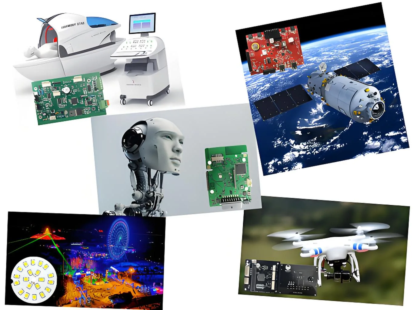
Downstream: Explosive Growth in PCB Applications
AI computing and smart EVs are reshaping PCB demand:
-
AI Servers: Drive higher PCB volumes/prices; increased compute density per rack + strict impedance control for AI chips
-
New Energy Vehicles (NEVs):
-
PCB content 4-5x traditional vehicles
-
800V platforms require 40% higher voltage resistance
-
ADAS sensors boost high-frequency PCB demand
-
-
الإلكترونيات الطبية: Implantable devices demand ionic contamination ≤1.56μg/cm² (NaCl eq.), far exceeding consumer standards.
02 Technology Breakthroughs: Three Critical Battles in Advanced PCB Manufacturing
PCB Material Revolution: From Basic Physics to Quantum Effects
High-frequency applications demand new materials. 5G base stations require ±7% impedance control (>10GHz), spurring novel resin R&د:
Material Science Formula: Df = ε” / ε’
(Dissipation Factor = Dielectric Loss / Permittivity)
Low-Df/Dk materials are pivotal. Industry benchmarks like modified PTFE (ص<0.001) and hydrocarbon resins (Df=0.001-0.002) reduce mmWave signal loss by over 60%.
PCB Process Innovation: Micron-Level Challenges
At UGPCB’s smart factory, laser drills process 8-layer 3+N+3 HDI at 300 holes/second. Key advances:
-
Any-layer Interconnect: Enables 15:1 aspect ratio microvias
-
السيطرة على المعاوقة: ± 5% التسامح (vs. ±7% for automotive radar)
-
Rigid-Flex Technology: Endures >100,000 bend cycles
Layer alignment within 12μm (1/6 human hair) ensures BGA voiding <25% (فئة IPC-A-610 3), preventing chip soldering failures.
Inspection Evolution: From Post-Production to Real-Time Prediction
AI-enhanced Automated X-ray Inspection (AXI) boosts BGA inspection speed 5x, reducing misses to <0.1%. Advanced failure analysis:
-
التفتيش البصري (100x microscope)
-
Electrical Testing (Network Analyzer)
-
X-ray/Cross-section (SEM/EDS)
-
Thermal Imaging (Hot spot detection)
Automotive-grade PCBs require -40°C~125°C thermal cycling (1,000 دورات) مع <0.01% impedance drift for BMS applications.
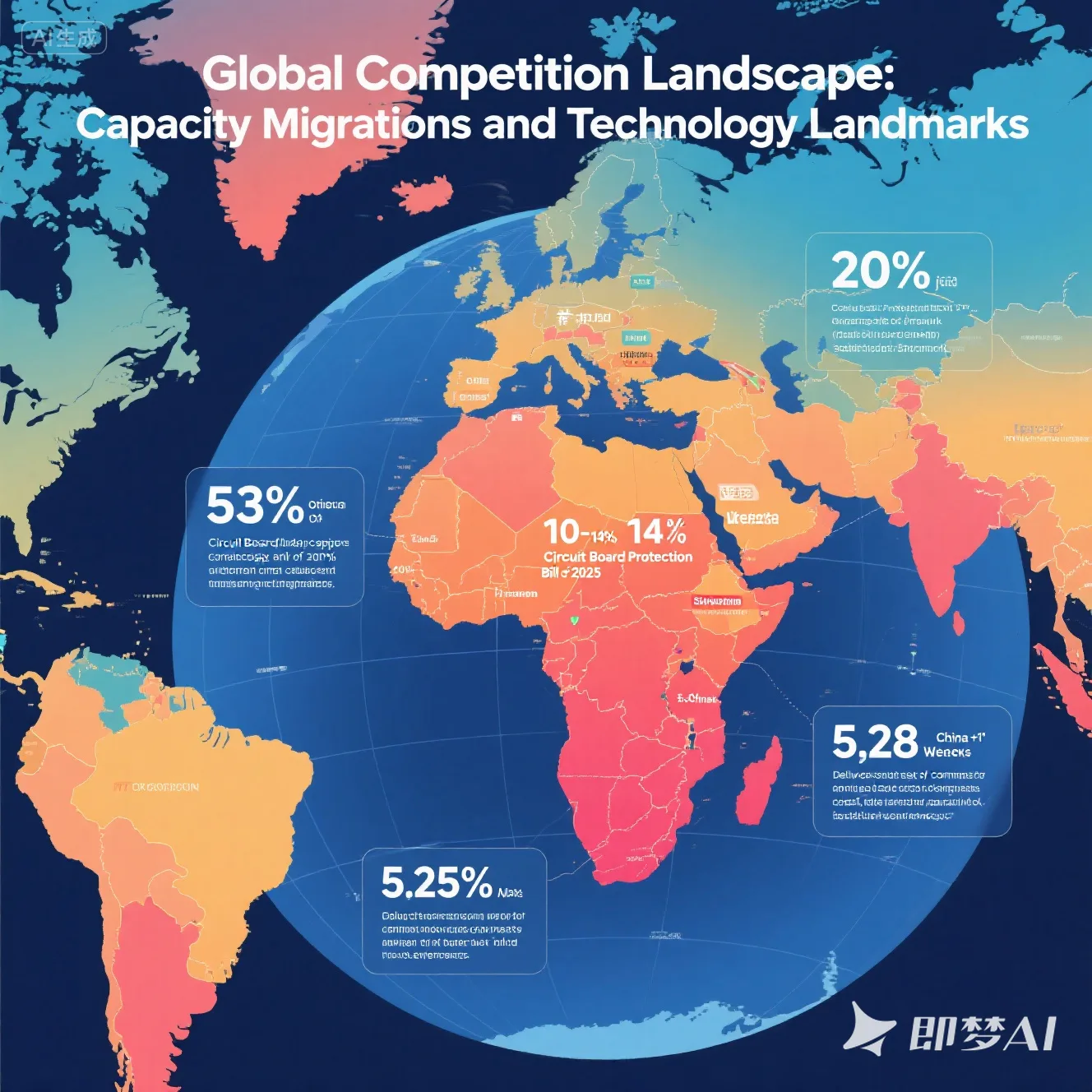
03 Global Competition: Capacity Shifts & Technology Positioning
Regional Dynamics: Asia-Pacific Dominance
2025 PCB landscape: “East-led, multi-polar growth”:
-
الصين: 53% global capacity (Prismark)
-
جنوب شرق آسيا: 20% YoY growth (Thailand, Vietnam)
-
USA: Subsidies via “Circuit Board Protection Act 2025”
China’s High-End PCB Ascent
While China leads in volume, its output remains mid-to-low tier (81% rigid boards). Leading firms are breaking barriers:
-
Shennan Circuits: FCBGA substrates for NVIDIA GPUs
-
UGPCB: Automotive-certified mmWave radar PCBs
-
Kinwong Electronics: SpaceX satellite communication PCBs
Research Nester projects the global PCB market reaching $155.38B by 2037, with China’s high-end share potentially rising from 15% ل 35%.
04 Future Battlefields: منظمة العفو الدولية & Electrification Drive Growth
AI Computing: ال “Dimensional Leap” for PCBs
AI infrastructure investment reshapes PCB tech:
-
AI Server Boards: >20 layers now comprise 60%
-
HBM Substrates: عرض الخط <8ميكرومتر
-
Optical Module PCBs: 80% low-loss material adoption
AI server PCB market CAGR: 16% (Frost & Sullivan). AI phones use 30% more layers and 15 FPCs/unit, accelerating HDI adoption.

EV Revolution: Reengineering the Automotive “Heart”
NEV electronics create new automotive PCB standards:
-
Domain Controllers: 8-12 layer HDI dominance
-
LiDAR Boards: High-frequency PTFE materials
-
800V Platforms: Insulation withstand ≥3kV
2025 NEV sales: ~15M units. PCB value/vehicle 4x ICE cars. BMS PCBs require 0.01% impedance stability (-40°C~125°C).
Sustainable Manufacturing: The Compliance Imperative
EU EPR regulations mandate:
-
100% lead-free solder by 2026
-
95% copper recycling rate
-
≥30% bio-based resins
China’s emission standards demand 40% VOC reduction, pushing water-based ink adoption in PCB printing from 35% ل 65% بواسطة 2027.
05 خاتمة: Strategic Positioning & Choices
The global PCB industry is undergoing deep transformation. Mordor Intelligence forecasts market growth from $84.24B (2025) to $106.85B (2030) في 4.87% CAGR. Key opportunities:
-
High-End Capacity: 18+ layer boards (9% CAGR), IC substrate shortage (30%)
-
Regional Shift: 25% lower setup costs in Southeast Asia
-
Material Innovation: Low Dk/Df materials (40% YoY demand growth)
Note: The data presented in this document is sourced from the latest reports of authoritative institutions including Prismark, IPC, and Frost & Sullivan. All technical parameters have been validated through rigorous testing conducted in CNAS-accredited laboratories. Process standards strictly adhere to current edition specifications such as IPC-6012EM* and IPC-2221B.
