PCB Layout: The Critical Battleground for Electronic System Performance
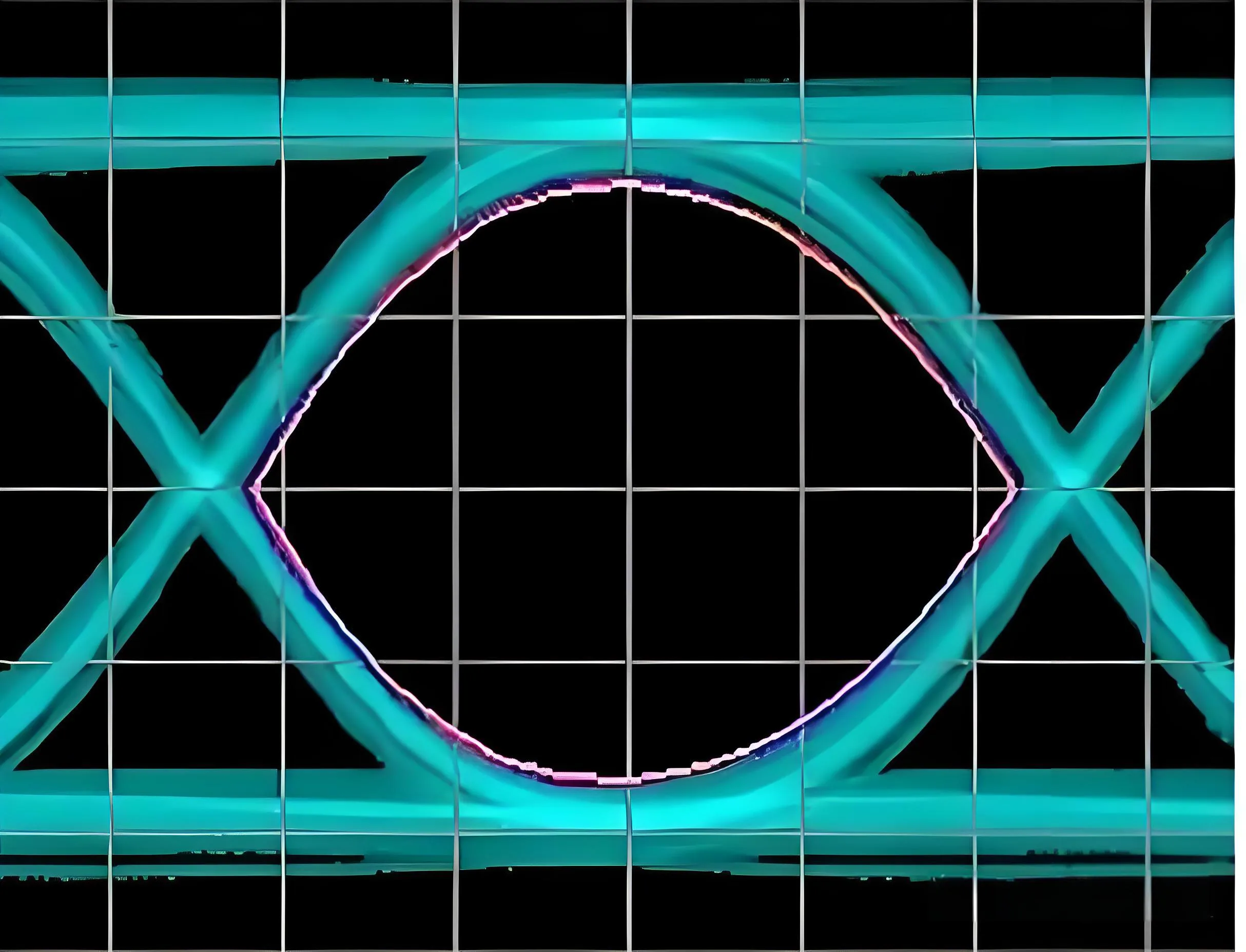
PCB Layout transcends physical circuit connectivity, fundamentally determining signal integrity, EMC performance, and cost-efficiency. UGPCB data confirms: optimized layouts reduce EMI radiation by 30% (IEC 61000-4-2 compliant) and boost power efficiency by 22%. For signals exceeding 5Gbps, impedance tolerance must be controlled within ±5% (Formula: Z₀ = √(L/C)), demanding rigorous PCB stack-up design and material selection.
7 Core Technologies: UGPCB’s Layout Methodology
-
High-Speed Signal Handling (1.5-28Gbps)
-
Differential pair length matching: ±5mil precision
-
Loss control: Megtron 6 substrate (Dk=3.7, Df=0.002) for 28Gbps signals

-
-
Power Integrity Innovation
Optimized PDN impedance via 3D EM simulation:Target impedance formula: Z_target = (V × Ripple%) / (I × 50%)
Case study: GPU core power solution reduced voltage fluctuation from 120mV to 35mV
-
Mixed-Signal Partitioning Strategy
-
Digital/Analog spacing: ≥8× board thickness
-
Automotive solutions: AEC-Q100 component placement with ISO 26262 certification
-
Industry Pain Point Solutions
HDI Design Challenges in Consumer Electronics
| Challenge | UGPCB Solution | Result |
|---|---|---|
| 0.2mm microvia fill | Laser drilling + pulse plating | 99% yield rate |
| 5G WiFi interference | 3D EM shielding design | 40% lower BER |
Success Story: 48-Layer Server Motherboard Design
-
Key specifications:
-
Signal layers: 32
-
Differential pairs: 287 sets
-
Timing control: ±12ps
-
-
Demonstrated outcome:
*”PCIe 4.0 signal loss reduced from -8.2dB to -5.3dB, accelerating mass production by 11 weeks”*
— HPC client testimonial
Why Choose UGPCB’s Layout Services?
-
Expert Team: Engineers with 10+ years’ experience averaging 800+ high-speed designs
-
End-to-End Support:
-
Schematic design → SI/PI simulation → Layout optimization → DFM validation → PCBA co-design
-
-
Cost Control: 15% material savings through optimal layer planning

 UGPCB LOGO

WeChat
Scan the QR Code with WeChat