
Mit der schnellen Entwicklung der 5G -Kommunikation, künstliche Intelligenz, und Hochgeschwindigkeits-Computertechnologien, Die Nachfrage nach überlegener thermischer Leistung in Leiterplatten (Leiterplatten) Für elektronische Geräte wird immer strengerer. Nach Prismark, Die globale Marktgröße für PCBs mit hohen Anforderungen an die thermische Dissipation soll erreichen $4.78 Milliarden in 2023, mit einem überschreitenden CAGR 9.2%. Vor allem im Bereich der Hochfrequenz und Hochgeschwindigkeits-PCBs, Lokalisierte Überhitzung ist zu einem kritischen Faktor geworden, der die Zuverlässigkeit der Geräte beeinflusst.
Technische Einschränkungen traditioneller eingebetteter Kupferblockprozesse
Der aktuelle Mainstream-Industrieprozess zum Einbetten von Kupferblöcken beinhaltet die Vorabwinnung der Kernkarte und Prepreg (Pp) vor Laminierung, Platzieren des Kupferblocks während des Laminierungsprozesses, und sich auf den Fluss des PP -Harzes stützen, um die Einbettung und Fixierung abzuschließen. Während diese Methode weit verbreitet ist, Es hat zwei signifikante Einschränkungen:
Erstens, Die in der Laminierung verwendete PP muss einen ausreichenden Harzgehalt haben. Gemäß dem IPC-4101E-Standard, Hochrösender PP muss einen Harzgehalt von haben 68% ± 5%. Wenn das Harzvolumen nicht ausreicht, Das Entleerung erfolgt um den Kupferblockfüllbereich, erkennbare Lücken bilden.
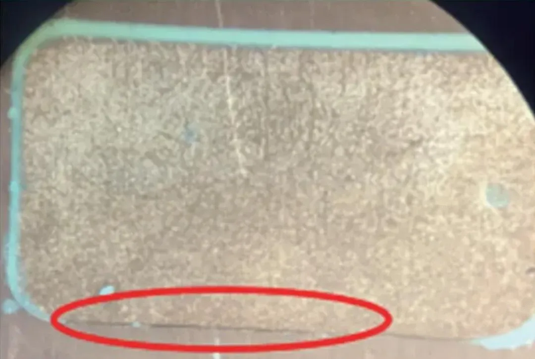

Zweitens, Der Fluss des PP muss genau kontrolliert werden. Laut IPC-TM-650 2.3.17 Testmethode, Die dynamische Viskosität von PP sollte im Bereich von kontrolliert werden 800-1,500 Pa · s (bei 180 ° C.). Wenn der Fluss zu hoch ist, Übermäßiges Harz kann in die Spaltbereiche fließen, Harzhunger in nahe gelegenen Leiterregionen verursachen, was zu schlechten Laminierung und inneren Rissen im Board führt (Figur 2).

Diese Einschränkungen machen traditionelle Methoden für nicht geeignet für HDI Produkte, die unter Verwendung sequentieller Aufbaulamination hergestellt werden. Um diese Branchenherausforderung anzugehen, Die Vakuumharzfüllungsmethode ist entstanden.
Prozessprinzip und technische Vorteile der Vakuumharzfüllung
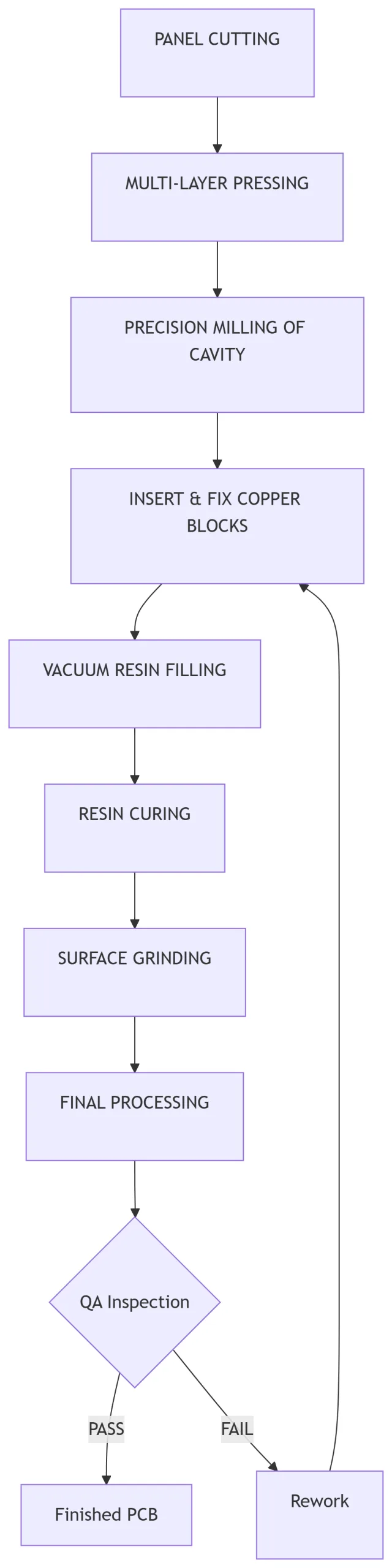
Die Vakuumharzfüllmethode verwendet einen völlig anderen technischen Ansatz: Erste, Präzisionsrouting wird am laminierten Board durchgeführt, um Hohlräume zu schaffen; Kupferblöcke werden dann platziert und befestigt; gefolgt von einer Harzfüllung unter Vakuumbedingungen; Nach Härtenhärtung, Der letzte Schritt ist das Schleifen. Der vollständige Verarbeitungsfluss ist: Pensionierung → Laminierung → Routing → Kupferblockplatzierung → Harzfüllung → Schleifen → nachfolgende Prozesse.

Diese Methode bietet erhebliche Vorteile gegenüber dem traditionellen Prozess:
-
Anwendbar auf komplexe Strukturen wie HDI -Boards
-
Einheitlichere und zuverlässigere Füllungsergebnisse
-
Fähigkeit zur Überarbeitung und Reparatur
-
Etwa 30% Verbesserung der Produktionseffizienz
-
Kostensenkung von ungefähr 15-20%
Entwurf und Validierung des Schlüsselparameters für den Vakuumfüllungsprozess
Hohlraumform und Größenoptimierungsdesign
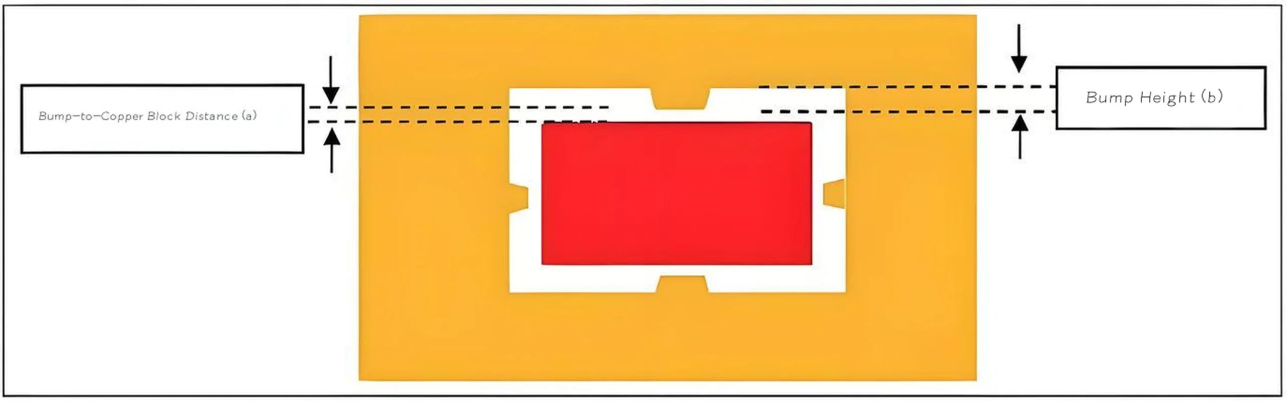
Gemäß strengen Anforderungen eines großen Kunden, Das Harzfüllgröße um den Kupferblock muss weniger als 0,254 mm betragen. Berücksichtigung der Genauigkeit der internen Routing -Maschine von ± 0,075 mm, Das Design der Hohlraumgröße muss befriedigen: 2A + B ≤ 0,179 mm (oder 2a + B ≤ 0,204 mm). Folglich, Vier Hohlraumgrößenschemata wurden entworfen:
① A = 0,05 mm, B = 0,050 mm
② A = 0,05 mm, B = 0,075 mm
③ A = 0,05 mm, B = 0,100 mm
④ A = 0,075 mm, B = 0,050 mm
Es wurden auch drei Hohlraumformkonstruktionen getestet:
-
Form a: Standard -Rechteck
-
Form b: Rechteck mit einem Vorsprung, der im Mittelpunkt jeder Seite hinzugefügt wurde
-
Form c: Rechteck mit einem Vorsprung, der auf allen vier Seiten 1 mm von jeder Ecke hinzugefügt wurde

Verwenden von Testplatten mit einer Dicke von 1,00 mm und Kupferblöcken mit einer Dicke von 0,98 mm, mit hochtemperaturbeständigem Klebeband befestigt, Auf einer Vakuumfüllmaschine wurde eine Versuchsfüllung ohne Harzless durchgeführt. Die Ergebnisse zeigten, dass die Form c (Rechteck mit Eckvorsprüngen) bot die beste Anti-Rotation und Anti-Bewegungsleistung, und wurde zur anschließenden Validierung ausgewählt.
Kupferblock -Fixierfilmmaterialauswahl
Berücksichtigung der einfachen Fixierung und Entfernung von Kupferblocks und Entfernung, sowie thermische Stabilität während des Backens, Der Fixierfilm muss die Anforderungen für einen hohen Temperaturwiderstand und die angemessene Klebrigkeit erfüllen. Zwei Materialien wurden verglichen: PE-Film und hochtemperaturbeständiges Band.
-
Auf dem Film: Unzureichender Wärmewiderstand (max 150 ° C.), Anfällig für Verformungen während des Backens.
-
Hochtemperaturbeständiges Band: Temperaturen über 200 ° C stand, hat mäßige Klebrigkeit, und hinterlässt keine Rückstände beim Entfernen.
Experimentelle Ergebnisse zeigten deutlich, dass hochtemperaturbeständiges Band die optimale Wahl für den Einbettungsfilm des Kupferblocks ist.
Optimierung des Höhenunterschieds zwischen Kupferblock und Brettoberfläche
Für die Validierung wurden zwei Höhendifferenzschemata ausgelegt:
-
Schema 1: Kupferblock 20 μm höher als die Platineoberfläche
-
Schema 2: Kupferblock 40 μm höher als die Platineoberfläche
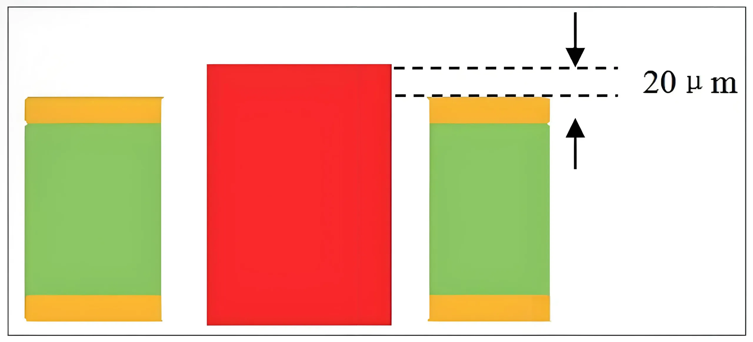

Experimentelle Ergebnisse zeigten keine Fehlanpassungsprobleme mit beiden Schema. Jedoch, Aus der Perspektive des nachfolgenden Schleifprozesses, Eine Höhenunterschiede von 20 μm ist für die Steuerung der Schleifmenge und die Verringerung der Prozesszeit förderlicher.
Harzfüllungsparameteroptimierung
Basierend auf der zuvor entworfenen Hohlraumgröße und -form, und unter Berücksichtigung der allgemein verwendeten internen Spezifikationen des Bildschirms der Bildschirme, Für Vakuumfüllung wurde ein 43 -t -Netz verwendet. Einpass- und Zwei-Pass-Füllschemata wurden entworfen. Der Harzfüllungseffekt im Kupferblockbereich wurde nach der Füllung inspiziert:
-
Einpassfüllung: Füllrate ca.. 85-90%, mit kleinen Blasen vorhanden.
-
Zwei-Pass-Füllung: Füllrate reicht über 98%, ohne offensichtliche Mängel.
Deutlich, Die Verwendung eines 43-t-Netzes für die Zweipass-Harzfüllung erfüllt die Harzvolumenanforderungen für den Kupferblockspaltbereich, Gewährleistung zuverlässiger Füllungsergebnisse.
Vergleichende Studie zu Backplatzierungsmethoden
Nach der Füllung von Harz, Das Aushärten backen ist erforderlich. Zwei Backplatzierungsmethoden waren intern erhältlich:
-
Vertikale Platzierung: Auf Rackträgern
-
Horizontale Platzierung: Beim Stapeln von Tabletts
Die experimentellen Ergebnisse zeigten deutlich, dass die vertikale Platzierung an Rack-Trägern nicht konform war. Der Hauptgrund ist, dass das gefüllte Harz während des Backens fließbar bleibt, und unter Schwerkraft, Es fließt nach unten, Harzverlust durch die Lücken verursachen und zu einer Hohlraumbildung führen. Die horizontale Platzierung auf Stapelschalen zeigte keine Anomalien und ist die empfohlene Backmethode.
Produktzuverlässigkeitsvalidierung und Testergebnisse
Basierend auf den Forschungsschlussfolgerungen aus den oben genannten wichtigsten Kontrollpunkten, Eine Menge eingebetteter Kupferblock-PCB-Produkte wurde durch Versuch produziert, Und 10 Die Proben wurden zufällig für umfassende Zuverlässigkeitstests ausgewählt. Testelemente enthalten:
Reflow -Lötentest
Gemäß IPC-6012E Standard, 6 Zyklen von Blei-freier Reflow-Löten (Spitzentemperatur 260 ° C.) wurden durchgeführt. Alle Proben wurden ohne Delaminierung bestanden, Blasenbildung, oder knacken.
Thermalspannungstest
Nach IPC-TM-650 2.6.8 Verfahren, Float -Lötentest bei 288 ° C ± 5 ° C wurde für durchgeführt 20 Sekunden. Alle Proben zeigten keine Anomalien.
Thermalradetest
Gemäß IPC-9701A Standard, 1000 Zyklen von -55 ° C bis 125 ° C wurden durchgeführt. Alle Proben haben die normale elektrische Leistung und strukturelle Integrität beibehalten.
Tisch: Zusammenfassung der Ergebnisse zu Zuverlässigkeitstests
| Testelement | Testbedingung | Passquote | Standardbasis |
|---|---|---|---|
| Reflow-Löten | 260° C × 6 Zyklen | 100% | IPC-6012E |
| Wärmespannung | 288° C × 20s | 100% | IPC-TM-650 2.6.8 |
| Thermalradfahren | -55° C ~ 125 ° C × 1000 Zyklen | 100% | IPC-9701A |
Anwendungsaussichten und kommerzieller Wert der Vakuumfüllungsmethode
Die Vakuumharzfüllungsmethode zum Einbetten von Kupferblöcken überwindet nicht nur die Einschränkungen der traditionellen Methoden, sondern bringt auch einen erheblichen kommerziellen Wert für die PCB -Branche.:
Umsetzung technischer Vorteile in den kommerziellen Wert
-
Verbesserte Ausbeute: Reduziert Schrott, die durch Entleerung und Risse verursacht werden, Erhöhung der Ausbeute ungefähr ungefähr 12-15%.
-
Kostensenkung: Vereinfacht den Prozessfluss, Reduzierung der Produktionskosten durch 15-20%.
-
Erweiterte Anwendungen: Ermöglicht die Verwendung der eingebetteten Kupferblockwärmeableitungstechnologie in HDI -Produkte, Neue Markträume öffnen.
Breite Anwendungsbereiche
Diese Technologie ist besonders geeignet für:
-
5G Basisstation Stromverstärker PCBs
-
Hochgeschwindigkeits-Server-Motherboards
-
Elektronische Steuereinheiten für Automobile (ABDECKUNG)
-
Hochleistungs-LED-Beleuchtungsbretter
-
Industrieleistungsmodule
Schlussfolgerung und Ausblick
Dieser Artikel bestätigt systematisch die Durchführbarkeit und Zuverlässigkeit der Vakuumharzfüllungsmethode in eingebetteten Kupferblock -PCB -Technologie durch Experimente. Die wichtigsten Schlussfolgerungen sind wie folgt:
-
Hohlraumform unter Verwendung eines Rechtecks mit Vorsprüngen 1 mm von jeder Ecke (Form c) verhindert effektiv Kupferblockbewegung und -drotation.
-
Verwenden von hochtemperaturbeständigem Band, wenn der Kupferblock-Fixierfilm die Effektivität der Fixierung gewährleistet und die anschließende Entfernung erleichtert.
-
Sowohl 20 & mgr; m als auch 40 & mgr; m Höhenunterschiede zwischen Kupferblock- und Brettdickungsmesswert sind machbar, Das 20 μM -Schema wird jedoch aus Sicht der Prozesskontrolle empfohlen.
-
Durch die Verwendung eines 43-t-Netzes für die Zweipassharzfüllung sorgt eine ausreichende und konsistente Füllung.
-
Horizontale Platzierung auf Stapelschalen während des Backen.

Im Vergleich zur traditionellen Laminierungsmethode zum Einbetten von Kupferblöcken, Die Vakuumharzfüllungsmethode bietet erhebliche Vorteile, einschließlich einer höheren Effizienz, geringere Kosten, höhere Nachbereitbarkeit, und Eignung für HDI -Boards. Da die Anforderungen an die thermische Dissipation in elektronischen Geräten weiter zunehmen, Diese neue Technologie ist bereit, eine entscheidende Prozessauswahl für die PCB -Fertigung mit hoher thermischer Dissipation zu werden.
Für Designingenieure und Beschaffungsspezialisten, die eine hohe Thermaldissipation -PCB -Lösungen suchen, Es wird empfohlen, detaillierte Diskussionen mit Profi zu führen PCB -Lieferanten. [Klicken Sie auf diesen Link Um den detaillierten Produktherstellungsbericht unseres Unternehmens herunterzuladen, um optimale Lösungen und technische Unterstützung zu erhalten, die auf bestimmte Anwendungen zugeschnitten sind.]
Qualitätsanbieter für hochwertige PCB Manufacturing -Dienstleister können umfassende Dienstleistungen von der Konstruktion bis zur Volumenproduktion bis hin zu anbieten Leiterplatte, Gewährleistung einer hervorragenden Produktleistung und Verkürzung von Zeit-to-Market.