


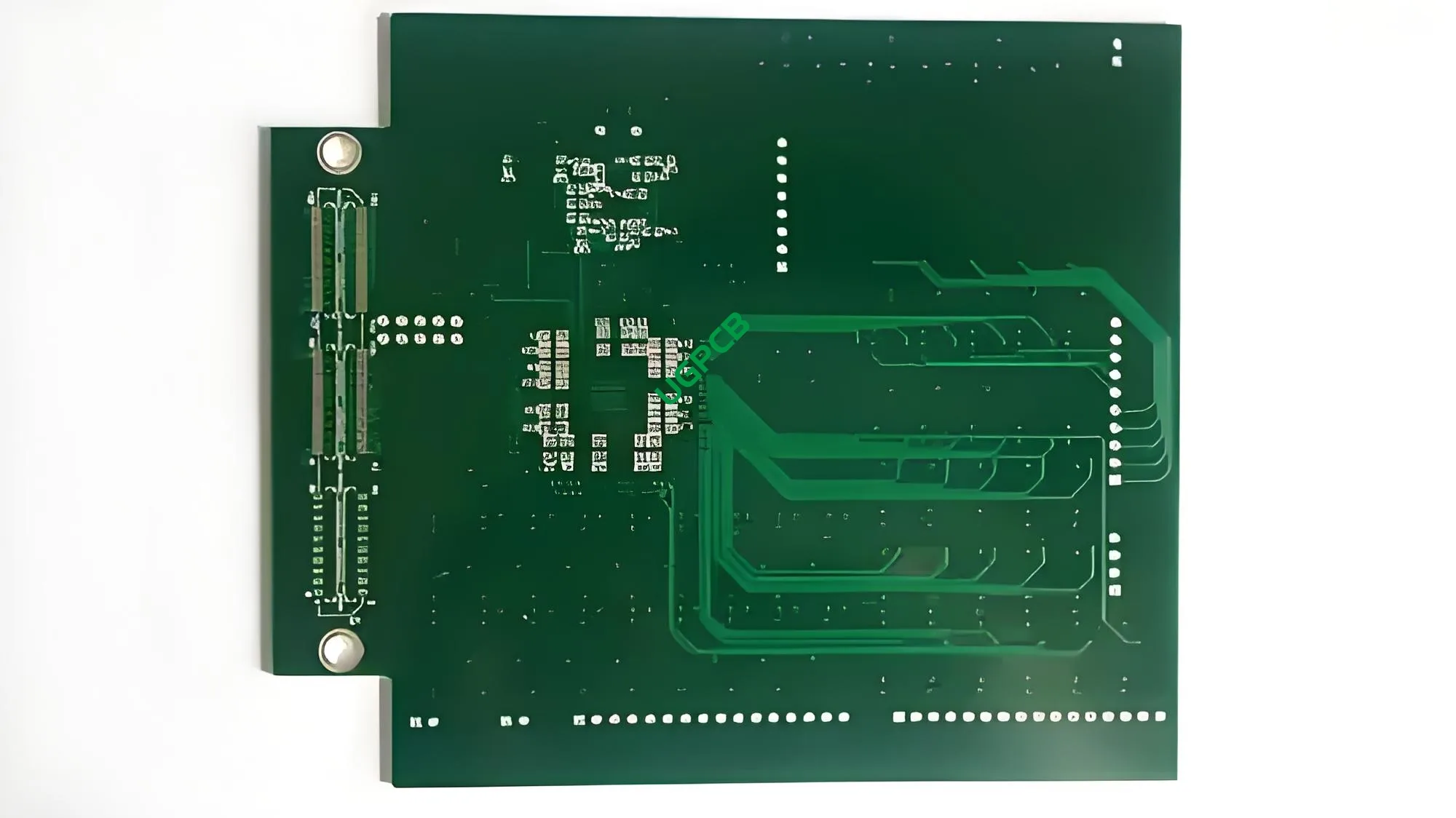
Was ist a 4 Layer PCB?
A 4-layer Printed Circuit Board (Leiterplatte) is an advanced elektronisches Bauteil that consists of four layers of conductive material, Typisch kupfer, getrennt durch Isolierschichten. This multilayer structure allows for complex circuit designs with high density and improved performance.

Entwurfsanforderungen
Designing a 4-layer PCB involves several key considerations:
- Material: Commonly made from FR-4, a composite material known for its excellent electrical properties and affordability.
- Schichtzahl: Wie der Name schon sagt, it has four layers, which can handle more complex circuitry compared to single or double-sided boards.
- Kupferdicke: Can range from 0.5OZ to 6OZ, depending on the application’s power requirements.
- Oberflächenbehandlung: Options include immersion gold, OSP (Bio -Lötlichkeitsschutz), and lead-free HASL (Heat Activated Solder Leveling), each offering different levels of solderability and protection.
- Spur und Raum: Minimum trace and space are typically set at 3mil (0.075mm), allowing for fine details in the circuit design.
Wie funktioniert es?
The 4-layer PCB functions by providing a platform where electronic components can be mounted and interconnected using conductive pathways etched into the copper layers. These pathways are separated by insulating layers, preventing electrical shorts while allowing signals to pass through via plated through-holes or vias.
Anwendungen
Aufgrund ihrer Komplexität und Zuverlässigkeit, 4-Schicht Leiterplatten are widely used in various consumer electronics including:
- Smartphones
- Tabletten
- Laptops
- Gaming consoles
- High-end audio equipment


Einstufung
4-layer PCBs can be classified based on several factors:
- Durch Material: Most commonly made from FR-4 due to its balance of cost, Stärke, und elektrische Eigenschaften.
- Durch Kupferdicke: Variiert von leichtem (0.5OZ) zum Schwergewicht (6OZ) Abhängig von den Anforderungen der Anwendung.
- Durch Oberflächenbehandlung: Options include immersion gold, OSP, and lead-free HASL, each offering different levels of protection and solderability.
Materialien verwendet
The primary materials used in manufacturing 4-layer PCBs include:
- FR-4: Ein mit Glas verstärkter Epoxidlaminat, der eine hervorragende mechanische Festigkeit und thermische Stabilität bietet.
- Kupfer: Wird für die leitenden Schichten verwendet, mit der Dicke variiert basierend auf den Entwurfsanforderungen.
- Lötmaske: Typically green, Weiß, Rot, or black, Es schützt die Kupferspuren vor Oxidation und versehentlichen Kurzkreisen.
- Surface Treatments: Such as immersion gold, OSP, or lead-free HASL, which improve solderability and protect against corrosion.
Leistungseigenschaften
Key performance attributes of a 4-layer PCB include:
- Hohe Dichte: Allows for more Komponenten to be packed into a smaller area.
- Zuverlässigkeit: Die Verwendung mehrerer Schichten verringert das Risiko elektrischer Shorts und verbessert die Signalintegrität.
- Signalintegrität: Aufgrund kürzerer Signalwege und reduziertem Übersprechen verbessert.
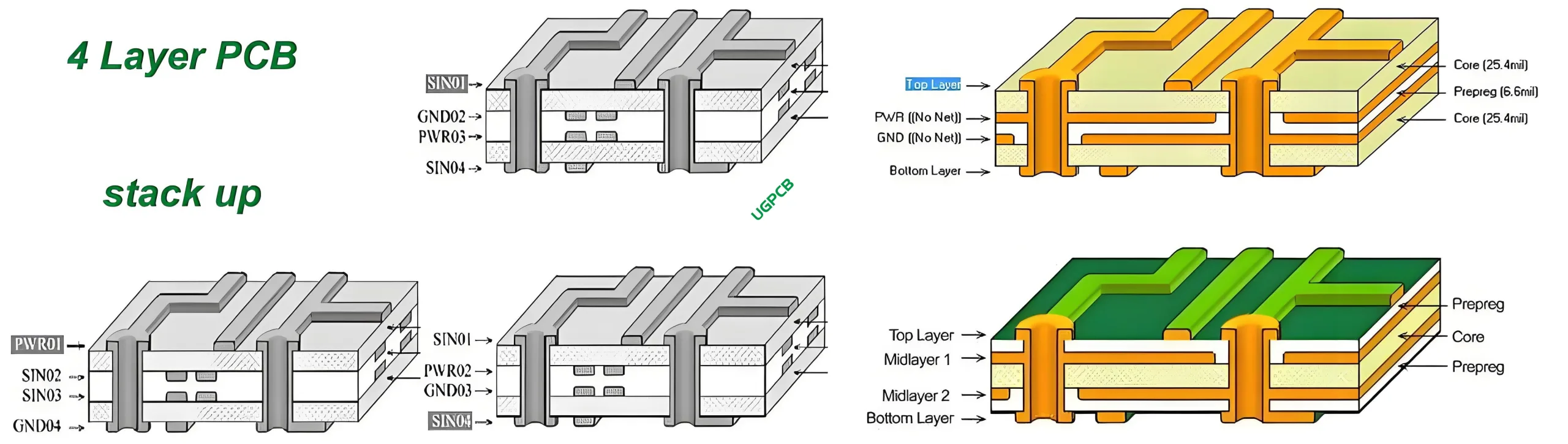
Strukturkomposition
Strukturell, a 4-layer PCB comprises:
- Leitfähige Schichten: Aus Kupfer gemacht, in die gewünschten Schaltungsmuster eingraviert.
- Isolierschichten: Elektrische Shorts zwischen leitenden Schichten verhindern.
- Plattierte Durchlögelvias: Erleichterung von Verbindungen zwischen verschiedenen Schichten.

Unterscheidungsmerkmale
Some notable features of a 4-layer PCB are:
- Feiner Tonhöhe: Allows for high-density interconnects, making it ideal for compact devices.
- Robustheit: Die Verwendung mehrerer Schichten liefert eine starke mechanische Bindung zwischen Board und Komponenten.
- Vielseitigkeit: Geeignet für eine Vielzahl von Anwendungen aufgrund anpassbarer Schichtzahlen und Materialauswahl.
Produktionsprozess
The manufacturing process of a 4-layer PCB involves several steps:
- Design und Layout: Verwenden von speziellen Software zum Erstellen des Schaltungsmusters.
- Materialvorbereitung: Schneiden von Grundmaterialien zu Größe und Reinigungsflächen.
- Laminierung: Stapeln und Binden einzelner Schichten unter Wärme und Druck.
- Radierung: Entfernen Sie überschüssiges Kupfer, um die gewünschten Schaltungswege zu bilden.
- Überzug: Hinzufügen einer dünnen Metallschicht zu Vias und exponierten Kupferbereichen.
- Lötmaskenanwendung: Applying the green, Weiß, Rot, or black coating to protect traces.
- Oberflächenbehandlung: Applying immersion gold, OSP, or lead-free HASL for solderability.
- Endinspektion: Sicherstellung von Qualität und Funktionalität vor dem Versand gewährleisten.
Anwendungsfälle
Common scenarios where a 4-layer PCB might be employed include:
- High-density interconnect applications in mobile devices.
- Fortgeschrittene Kommunikationssysteme, die einen niedrigen Signalverlust erfordern.
- Tragbare medizinische Instrumente, die zuverlässige Leistung in harten Umgebungen benötigen.
- Automobilelektronik, die Robustheit und Langlebigkeit fordert.
Zusammenfassend, the 4-layer PCB represents a significant advancement in Leiterplatte Technologie, offering unparalleled complexity and performance for modern electronic applications. Its design flexibility combined with superior signal integrity and durability makes it an essential component in the development of next-generation consumer electronics and beyond.